Check patentability & draft patents in minutes with Patsnap Eureka AI!

Fin type field effect transistor and formation method thereof

A fin field effect and transistor technology, which is applied in the fields of semiconductor devices, semiconductor/solid-state device manufacturing, electrical components, etc., can solve problems such as difficulty in adjusting the threshold voltage of fin field effect transistors

Active Publication Date: 2015-02-11
SEMICON MFG INT (SHANGHAI) CORP
View PDF5 Cites 2 Cited by
  • Summary
  • Abstract
  • Description
  • Claims
  • Application Information

AI Technical Summary

Problems solved by technology

[0005] When the existing fin field effect transistors are in use, the bias control voltage is usually connected to the semiconductor substrate 10 to adjust the threshold voltage of the fin field effect transistors, but the existing adjustment methods have no effect on the fin field effect transistors. It is difficult to adjust the threshold voltage of the transistor

Method used


Image

  • Fin type field effect transistor and formation method thereof
  • Fin type field effect transistor and formation method thereof
  • Fin type field effect transistor and formation method thereof

Examples


Embodiment Construction

[0033] As mentioned in the background art, it is difficult to adjust the threshold value of the fin field effect transistor by using the substrate bias voltage in the prior art.

[0034] refer to figure 1 In the prior art, when adjusting the threshold voltage of the fin field effect transistor, the bias control voltage Vb is usually connected to the semiconductor substrate 10. Research has found that the bias control voltage Vb needs to pass through the semiconductor substrate 10 and the fin portion 14 Only then can it be conducted to the vicinity of the surface of the fin 14 at the bottom of the gate structure 12. Due to the high height of the fin 14, the conduction path of the bias control voltage Vb is very long, and the resistance on the conduction path is relatively large. Therefore, through the bias control The potential of the voltage Vb applied to the surface of the fin 14 at the bottom of the gate structure 12 is very small, which is not conducive to the adjustment of...


PUM

PropertyMeasurementUnit
Thicknessaaaaaaaaaa
Thicknessaaaaaaaaaa
Thicknessaaaaaaaaaa

Abstract

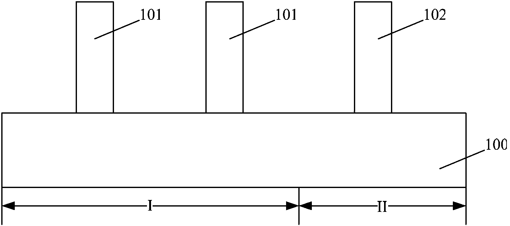
The invention discloses a fin type field effect transistor and a formation method thereof. The fin type field effect transistor formation method comprises steps that a semiconductor substrate is provided, and the semiconductor substrate comprises a first region and a second region; a first fin portion is formed at the first region, and a second fin portion is formed at the second region; a first medium layer is formed at the surface of the semiconductor substrate, the surface of the first medium layer is lower than top faces of the first fin portion and the second fin portion; a transition layer is formed at the surface of the first fin portion to cover a part of a side wall of the first fin portion and a part of the surface of the top portion, the oxidation rate of the transition layer is greater than the oxidation rate of the material of the second fin portion; oxidation treatment on the transition layer is carried out, and the oxidation layer is oxidized to form a first interface layer; and a first grid structure crossing the first fin portion and a second grid structure crossing the second fin portion are formed at the surface of the first interface layer. Through the fin type field effect transistor formation method, transistors having different threshold voltages can be conveniently formed.

Description

technical field [0001] The invention relates to the technical field of semiconductors, in particular to a fin field effect transistor and a forming method thereof. Background technique [0002] With the continuous development of semiconductor process technology, the process node is gradually reduced, and the gate-last (gate-last) process has been widely used to obtain an ideal threshold voltage and improve device performance. However, when the feature size (CD, Critical Dimension) of the device is further reduced, even if the gate-last process is adopted, the structure of the conventional MOS field effect transistor can no longer meet the requirements for device performance. Fin field effect transistor (Fin FET) as Substitution of conventional devices has received extensive attention. [0003] At the same time, the integration level of the chip is getting higher and higher, and the scale is getting bigger and bigger. A single chip usually includes a core logic transistor ar...

Claims


Application Information

Patent Timeline
IPC IPC(8): H01L21/336H01L29/78
CPCH01L29/06H01L29/66795H01L29/785
Inventor 三重野文健
Owner SEMICON MFG INT (SHANGHAI) CORP
Features
  • R&D
  • Intellectual Property
  • Life Sciences
  • Materials
  • Tech Scout
  • Unparalleled Data Quality
  • Higher Quality Content
  • 60% Fewer Hallucinations
Learn More