Power semiconductor device and manufacturing method thereof

A technology of power semiconductors and manufacturing methods, which is applied in the direction of semiconductor devices, semiconductor/solid-state device manufacturing, transistors, etc., can solve the problems of reduced breakdown voltage, instability, and large leakage current, so as to reduce leakage current, stabilize surface electric field, Effect of Enhanced Voltage Reliability

Active Publication Date: 2015-02-11
CSMC TECH FAB2 CO LTD
View PDF6 Cites 1 Cited by
  • Summary
  • Abstract
  • Description
  • Claims
  • Application Information

AI Technical Summary

Problems solved by technology

[0009] Based on this, it is necessary to provide a new solution to the phenomenon that the leakage current of the devices of the existing planar terminal technology is too large or even

Method used


Image

  • Power semiconductor device and manufacturing method thereof
  • Power semiconductor device and manufacturing method thereof
  • Power semiconductor device and manufacturing method thereof

Examples


Embodiment Construction

[0063] Before explaining the technical solutions provided by the present invention in detail, the technical vocabulary involved in this embodiment will be explained first.

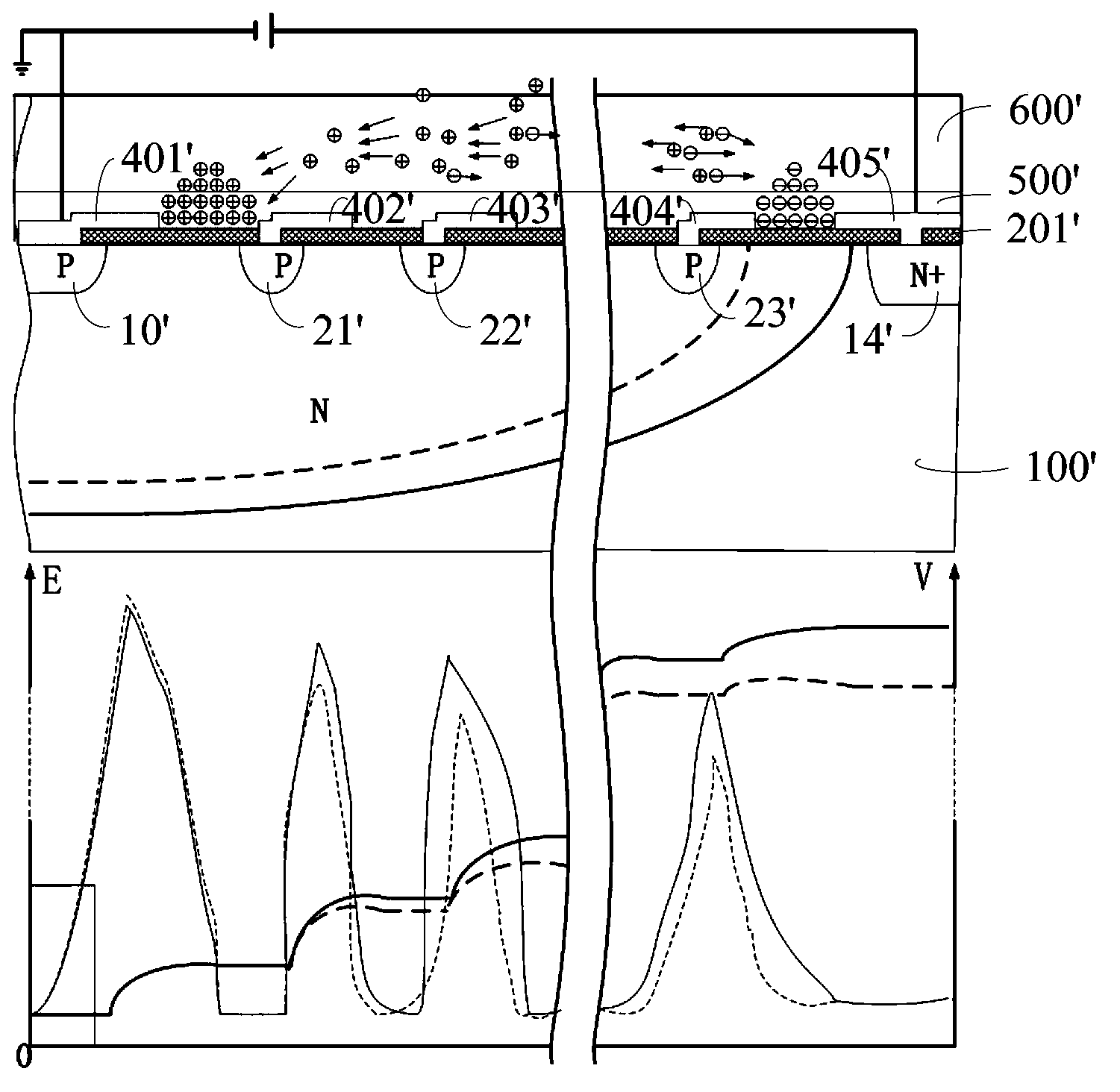
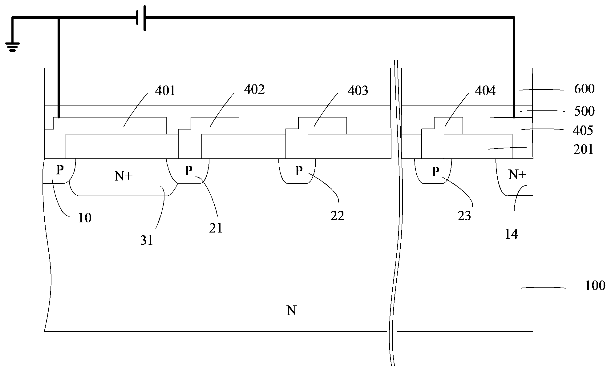
[0064] The power device includes two parts, the device area and the terminal area, wherein the device area realizes the basic functions of the power device, and the terminal area realizes the breakdown voltage of the power device.

[0065] Generally, the end region is doped to form a ring to achieve the withstand voltage of the power device. The doped region opposite to the substrate doping type formed at the edge of the device region is the main junction region, also known as the equipotential ring (similar to the device region Surface equipotential, equivalent to 0V).

[0066] The impurity opposite to the substrate is diffused at the edge of the device region to form the main junction region to form a PN junction (main junction) with the substrate, and a ring with the same doping as the main junction reg...


PUM

PropertyMeasurementUnit
Thicknessaaaaaaaaaa

Abstract

Provided is a power semiconductor device and a manufacturing method thereof. The power semiconductor device comprises a first doping type semiconductor substrate which is provided with a device area. A second doping type main junction area and multiple field limiting rings are formed at the edge of the device area. The first doping type and the second doping type are opposite. A first doping area is formed in the semiconductor substrate arranged between the main junction area and the first field limiting ring adjacent to the main junction area. The doping type of the first doping area is the same with that of the semiconductor substrate, and doping density is higher than that of the semiconductor substrate. In the semiconductor power device, surface concentration of the semiconductor substrate between the main junction area and the first field limiting ring is increased by the first doping area between the main junction area and the first field limiting ring. Influence on the electric field caused by field plate accumulation of movable charges on the main junction area under the high-temperature and high-voltage condition can be effectively reduced due to high electronic potential.

Description

technical field [0001] The invention relates to the technical field of semiconductors, in particular to a power semiconductor device and a manufacturing method thereof. Background technique [0002] The basic requirement of modern power semiconductor devices is to be able to withstand high voltage and high current operation. Among them, the silicon-based power MOSFET usually forms a MOS power semiconductor device with a large aspect ratio by connecting a large number of MOS units in parallel to ensure that the surface voltage between the parallel MOS units in the middle of the large part is roughly the same. However, the voltage between the MOS unit at the boundary (ie terminal) and the surface of the substrate is very different, which often causes the surface electric field to be too concentrated, and due to the curvature effect of the planar junction, the junction bending part of the PN junction at the boundary and the electric field at the surface Increase, causing the e...

Claims


Application Information

Patent Timeline
IPC IPC(8): H01L27/088H01L29/06H01L29/40H01L21/8234H01L21/28
Inventor 钟圣荣王根毅邓小社周宏伟
Owner CSMC TECH FAB2 CO LTD
Why Eureka
Try Eureka