
Eureka
For R&D, Eureka makes reading and utilizing patents & technical documents easy.
Eureka AIR
Designed for self-driven R&D workflows. Generate viable solutions, solve complex R&D challenges, empower your innovation with AI.

Eureka Materials
Designed for material experts only. Revolutionize your material R&D, from search, analyze, to developing new materials.

TechResearch
Generate reliable direction feasibility study reports for your R&D in just a few steps.

TechSeek
Discover and master advanced knowledge NOW. Basics, ideas, possibilities, all at once.

TechMind
As an expert in R&D Theories, TechMind can generates customized viable solutions instantly.

TechRisk
Analyze your overall solution with one click, know your potential R&D risks in advance.

TechMonitor
Get weekly tech updates, stay abreast of the latest tech innovations and key insights.
Back lighting type image sensor structure capable of improving saturation throughput
An image sensor, back-illuminated technology, applied in the field of image sensors, can solve the problems of low pixel signal saturation capacity and small pixel area, and achieve the effect of improving signal saturation capacity and improving potential well potential swing
- Summary
- Abstract
- Description
- Claims
- Application Information
AI Technical Summary
Problems solved by technology
Method used
Image

Examples
specific Embodiment approach
[0016] The preferred embodiment of the structure of the back-illuminated image sensor with improved saturation capacity of the present invention is:
[0017] It includes a logic circuit and a pixel array placed in a semiconductor substrate, an N-type ion ring is arranged in the semiconductor substrate around the pixel array region, and a P-type ion ring is arranged between the pixel array region and the N-type ion ring .
[0018] The N-type ionic ring runs through the thickness of the semiconductor substrate, its upper surface is the front of the substrate, and its lower surface is the back of the substrate, and the width of the N-type ionic ring in the semiconductor substrate is greater than or equal to 0.2um.
[0019] The depth of the P-type ion ring in the semiconductor matrix is greater than or equal to 0.2um, and the width is greater than or equal to 0.2um.
[0020] The distance between the N-type ion ring and the P-type ion ring is greater than or equal to 0um.
[00...
specific Embodiment
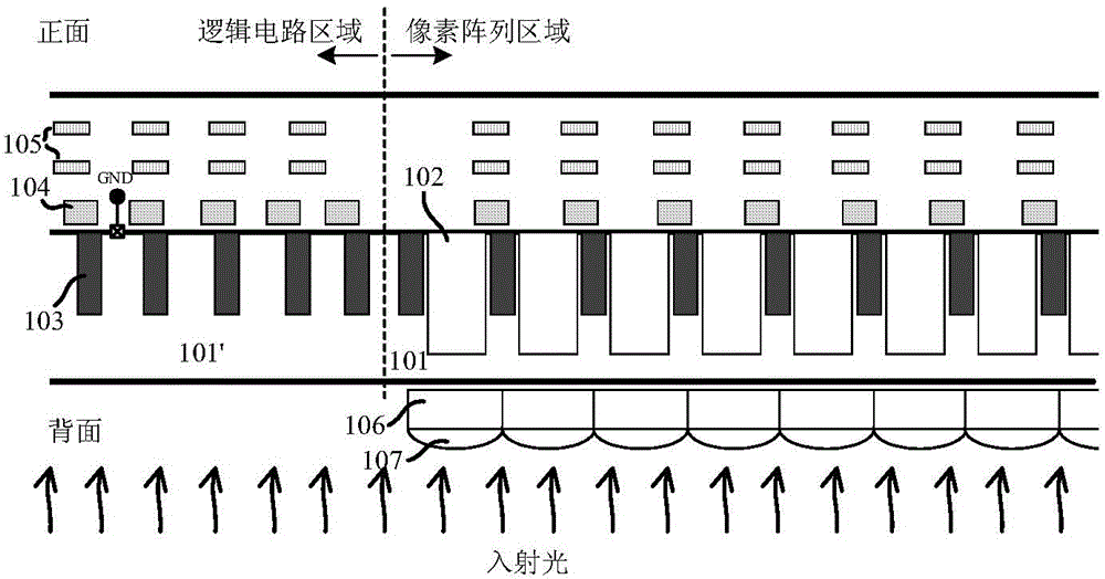
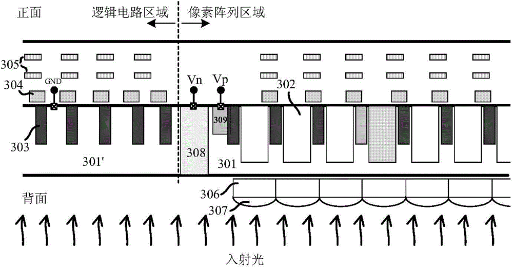
[0025] Schematic diagram of the sectional structure of the back-illuminated image sensor structure with improved saturation capacity of the present invention, as shown in image 3 shown. image 3 Among them, 301 is the semiconductor base in the pixel array area, 301' is the semiconductor base in the logic circuit area, 302 is the photodiode, 303 is the shallow trench isolation area, 304 is the polysilicon gate of the transistor device, 305 is the metal interconnection line, 306 is The color filter on the back side, 307 is the microlens on the back side, 308 is the N-type ion ring, and 309 is the P-type ion ring; wherein, Vn is the external potential of the N-type ion ring 308, and Vp is the external connection of the P-type ion ring 309 potential, GND is the external potential of the semiconductor substrate 301' in the logic circuit region.
[0026] A schematic plan view of the structure of the back-illuminated image sensor with improved saturation capacity of the present inv...
PUM
 Abstract
Description
Claims
Application Information
 - R&D Engineer
- R&D Manager
- IP Professional
- Industry Leading Data Capabilities
- Powerful AI technology
- Patent DNA Extraction
Browse by: Latest US Patents, China's latest patents, Technical Efficacy Thesaurus, Application Domain, Technology Topic, Popular Technical Reports.
© 2024 PatSnap. All rights reserved.Legal|Privacy policy|Modern Slavery Act Transparency Statement|Sitemap|About US| Contact US: help@patsnap.com