Broadband full-port matched waveguide power distributing/combining method

An all-port and waveguide technology, which is applied in the field of broadband all-port matching waveguide power division and synthesis, can solve the problems of poor stability, narrow space in the waveguide, and difficulty in application, and achieve good stability.

Inactive Publication Date: 2015-02-18
THE 41ST INST OF CHINA ELECTRONICS TECH GRP
View PDF2 Cites 8 Cited by
  • Summary
  • Abstract
  • Description
  • Claims
  • Application Information

AI Technical Summary

Problems solved by technology

The advantage of this structure is that it is compact, but its biggest disadvantage is that the space in the waveguide is very small in the millimeter wave band, and the number of stacked layers is very limited. Therefore, this structure cannot achieve multiple Road power distribution and combination
In order to achieve multi-channel power distribution and synthesis, the radial waveguide power division and synthesis scheme is generally adopted. The electromagnetic wave first enters the broadband radial waveguide from the coaxial, and then enters the rectangular waveguide from the radial waveguide to complete the power distribution. Each signal entering the rectangular waveguide Enter the microstrip plane circuit through the rectangular waveguide-microstrip probe array conversion structure, and then complete the multi-channel power distribution and synthesis, but this structure uses the coaxial as a transmission medium for multi-channel power division, as the frequency enters In the frequency band of 5 mm ...

Method used


Image

  • Broadband full-port matched waveguide power distributing/combining method

Examples


Embodiment 1

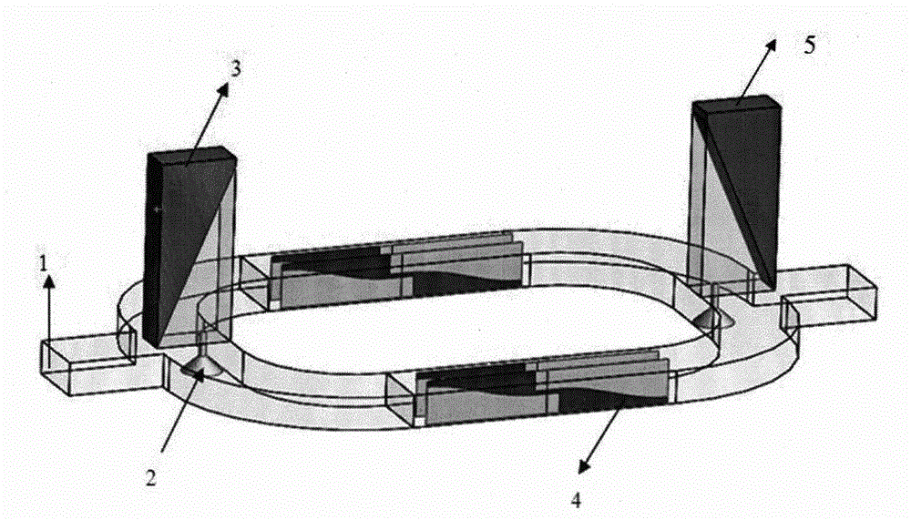
[0029] Such as figure 1 As shown, the power distribution / combination structure designed in the present invention, in this structure, the electromagnetic wave is first input by the input waveguide 1, and the input signal enters multiple channels with equal amplitude and the same direction under the joint action of the inductive diaphragm 2 and the absorbing load 3. Layer Power Allocation Structure4. The signal in 4 passes through multi-layer gradient fin lines to realize spatial power distribution and synthesis, and the synthesized signal is output through the output waveguide 5 .

[0030] By rationally designing the size of the inductive diaphragm 2 and the absorbing load, the broadband port matching between the waveguide power division unit and the spatial multilayer power distribution / combination unit can be realized, thereby improving the stability of the synthesized amplifier based on this structure.

[0031] By rationally designing the inductance diaphragm 2, absorbing l...

Embodiment 2

[0034] On the basis of the above examples, if figure 1 As shown, further, the electromagnetic wave is first input 1 through the input waveguide, and the input signal enters the multilayer power distribution structure 4 with equal amplitude and same direction under the joint action of the inductive diaphragm 2 and the absorbing load 3 . The signal in 4 passes through multi-layer gradient fin lines to achieve spatial power distribution and synthesis, and the synthesized signal is output 5 through the output waveguide.

[0035] By rationally designing the sizes of the inductive diaphragm 2 and the absorbing load 3, the broadband port matching between the waveguide power division unit and the spatial multilayer power distribution / combination unit can be realized, thereby improving the stability of the synthesized amplifier based on this structure.

[0036] By rationally designing the inductance diaphragm 2, absorbing load 3, gradient equation and position 4 of the opposite pole fi...

Embodiment 3

[0039] On the basis of the above examples, if figure 1 As shown, a broadband full-port matching waveguide power division and synthesis method is provided, which includes the following steps:

[0040] A: The electromagnetic wave is input by the input waveguide;

[0041] B: The signal enters the multi-layer power distribution structure through the combined action of the inductive diaphragm and the absorbing load;

[0042] C: Through the multi-layer impedance gradient fin line, the spatial power distribution and synthesis signal are realized;

[0043] D: The synthesized signal is output by the output waveguide.

[0044] On the basis of the above embodiments, wherein, in the step B, the signals enter the multi-layer power distribution structure with equal amplitude and the same direction.

[0045] On the basis of the above embodiment, wherein the input waveguide is provided with a waveguide power division unit, so as to realize waveguide power division of electromagnetic waves. ...


PUM

PropertyMeasurementUnit
Impedance valueaaaaaaaaaa

Abstract

A broadband full-port matched waveguide power distributing/combining method includes the steps that A, electromagnetic wave is input through an input waveguide and formed into an input signal; B, under combined action of an inductance diaphragm and an absorbing load, the signal enters a multi-layer power distribution structure; C, through multi-layer impedance gradient fin line, the space power distribution combining signal is achieved; D, the combining signal is output through an output waveguide. According to the arrangement, wide-band high-frequency efficient multi-path and fine all-port is matched, within millimeter wave frequency band, working band width reaches full band width of the waveguide, combing efficiency reaches more than 80%, frequency range is applicable to 170GHz, and an amplifier, based on the full-port matching technique, is good in stability.

Description

technical field [0001] The invention relates to a synthesis method, in particular to a broadband full-port matching waveguide power division synthesis method. Background technique [0002] As an important part of millimeter-wave radar, guidance and communication systems, millimeter-wave solid-state power amplifiers have become an important topic in the field of microwave and millimeter-wave research. With the continuous improvement of the output power requirements of the amplifier, the output power of a single amplifier chip can no longer meet the needs of the system. Therefore, the technology of multi-channel amplification and power combination must be used to effectively improve the output power of the entire amplifier circuit. [0003] Power distribution / combiners are mainly divided into planar and space forms. Planar circuit combiners and waveguide-based space power combiners. As the frequency increases, the insertion loss of planar circuit power dividers is relatively l...

Claims


Application Information

Patent Timeline
IPC IPC(8): H01P5/12
Inventor 邓建钦姜万顺王明超
Owner THE 41ST INST OF CHINA ELECTRONICS TECH GRP
Why Eureka
Try Eureka