VCSEL array packaging structure based on optical encapsulation process and high-power VCSEL laser device of VCSEL array packaging structure

An array packaging and laser technology, applied in lasers, laser parts, semiconductor lasers, etc., can solve problems such as affecting the appearance and structure, complex and cumbersome, and achieve the effect of improving transmittance, avoiding heat, and reducing interface incident loss.

Inactive Publication Date: 2015-02-18
SANHE LASERCONN TECH CO LTD
View PDF5 Cites 5 Cited by
  • Summary
  • Abstract
  • Description
  • Claims
  • Application Information

AI Technical Summary

Problems solved by technology

This sealing method is often very complicated and cu

Method used


Image

  • VCSEL array packaging structure based on optical encapsulation process and high-power VCSEL laser device of VCSEL array packaging structure
  • VCSEL array packaging structure based on optical encapsulation process and high-power VCSEL laser device of VCSEL array packaging structure
  • VCSEL array packaging structure based on optical encapsulation process and high-power VCSEL laser device of VCSEL array packaging structure

Examples


Embodiment Construction

[0025] The technical content of the present invention will be described in detail below in conjunction with the accompanying drawings and specific embodiments.

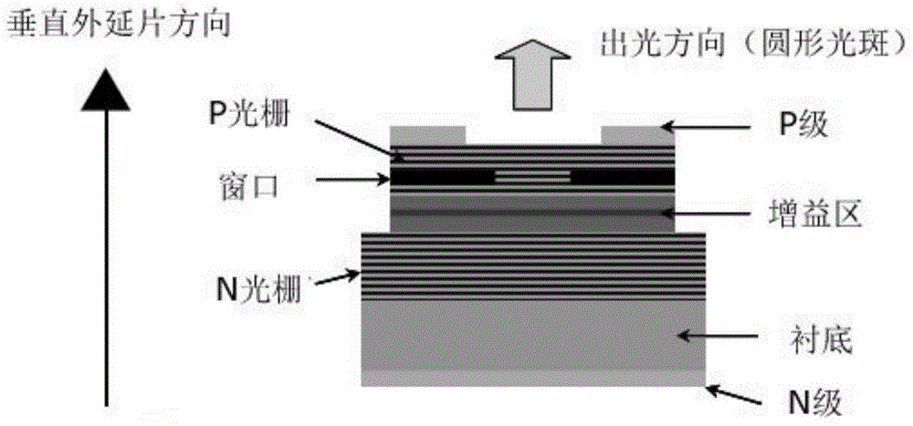
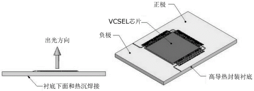
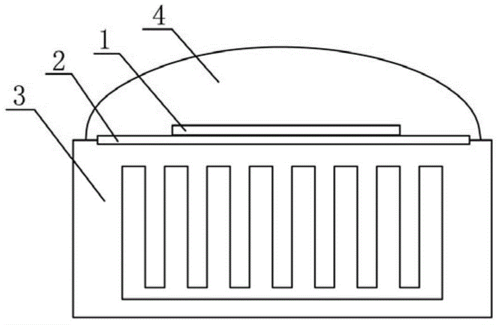
[0026] Such as image 3 As shown, the VCSEL array packaging structure provided by the present invention includes a VCSEL array 1 , a substrate 2 and a laser heat sink 3 , wherein the VCSEL array 1 is packaged on the laser heat sink 3 through the substrate 2 . Specifically, the VCSEL chip is directly welded on the upper surface of the substrate 2 , and then the lower surface of the substrate 2 is welded on the laser heat sink 3 . The substrate 2 has good thermal conductivity, and the heat of the VCSEL array 1 can be conducted out in time through the substrate 2 and the laser heat sink 3 to realize heat dissipation and cooling of the VCSEL array 1 .

[0027] The optical encapsulant 4 is introduced for the first time in the packaging structure provided by the present invention. By directly covering, encapsulating and cu...


PUM


Abstract

The invention provides a VCSEL array packaging structure based on the optical encapsulation process and a high-power VCSEL laser device of the VCSEL array packaging structure. In the VCSEL array packaging structure, a VCSEL array is packaged on a laser device heat sink, the surface of the VCSEL array is covered with a layer of optical pouring sealant, and the VCSEL array is completely covered with the optical pouring sealant. By introducing the encapsulation process to the sealing process of the VCSEL laser device, the sealing problem of the VCSEL laser device is effectively solved. In addition, by adjusting the shape and the type of the optical encapsulation sealant, the interface incidence loss between a VCSEL chip and optical windows can be greatly reduced through the combination with different optical windows, and the transmittance of the laser device is further improved. Meanwhile, the high-thermal-conductivity optical encapsulation sealant has a certain heat conduction effect and a certain cooling effect on the optical windows at the same time, and the optical windows are prevented from heating under the high-power condition.

Description

technical field [0001] The invention relates to a VCSEL array packaging structure based on an optical potting process, and at the same time relates to a high-power VCSEL laser using the packaging structure, which belongs to the technical field of semiconductor lasers. Background technique [0002] In the field of semiconductor lasers, according to the relationship between the light emitting direction and the plane of the epitaxial wafer where the laser chip is located, lasers can be divided into two types: vertical cavity surface emitting laser (Vertical Cavity Surface Emitting Laser, VCSEL for short) and edge emitting semiconductor laser (Edge Emitting Laser Diode). . [0003] Among them, the vertical cavity surface emitting laser is a semiconductor laser whose light output direction is perpendicular to the epitaxial wafer. The structure of the vertical cavity surface emitting laser can be found in figure 1 The schematic diagram shown. The high-power VCSEL laser is a two-...

Claims


Application Information

Patent Timeline
IPC IPC(8): H01S5/183H01S5/022H01S5/024
Inventor 李阳李德龙
Owner SANHE LASERCONN TECH CO LTD
Why Eureka
Try Eureka