Unified bit width converting structure and method in cache and bus interface of system chip

A bus interface, bit width conversion technology, applied in memory systems, memory address/allocation/relocation, instruments, etc., can solve problems that have not yet been discovered, and achieve the effect of clear design structure, enhanced compatibility, and guaranteed consistency

Active Publication Date: 2015-02-25
NO 771 INST OF NO 9 RES INST CHINA AEROSPACE SCI & TECH
View PDF3 Cites 13 Cited by
  • Summary
  • Abstract
  • Description
  • Claims
  • Application Information

AI Technical Summary

Problems solved by technology

After searching the relevant literature, no method that can solve this problem has been found so far

Method used


Image

  • Unified bit width converting structure and method in cache and bus interface of system chip
  • Unified bit width converting structure and method in cache and bus interface of system chip
  • Unified bit width converting structure and method in cache and bus interface of system chip

Examples


Embodiment Construction

[0032] The present invention will be further described in detail below in conjunction with the accompanying drawings, which are explanations rather than limitations of the present invention.

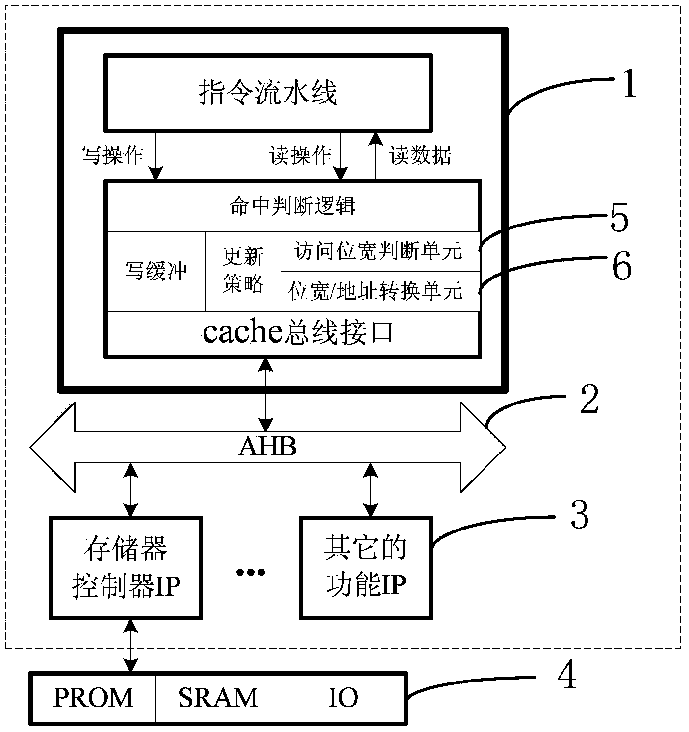
[0033] see figure 1 , the unified bit width conversion structure of the cache and the bus interface in the system chip of the present invention includes a processor core 1 and a plurality of IP cores 3 that perform data interaction with the processor core 1 through the on-chip bus 2, wherein the memory controller IP and the off-chip The main memory 4 is connected; the processor core 1 includes an instruction pipeline and a hit judgment logic unit capable of receiving instruction pipeline read / write operation instructions, and an access bit width judgment unit 5 and a bit width / bit width judgment unit 5 are arranged between the hit judgment logic unit and the cache bus interface. The address conversion unit 6 and the hit judgment logic unit can send the judgment result data to the instruc...


PUM


Abstract

The invention discloses a unified bit width converting structure and method in a cache and a bus interface of a system chip. The converting structure comprises a processor core and a plurality of IP cores carrying out data interaction with the processor core through an on-chip bus, and a memorizer controller IP is communicated with an off-chip main memorizer. The processor core comprises an instruction assembly line and a hit judgment logic unit receiving an operation instruction of the instruction assembly line. An access bit width judgment unit and a bit width/address converting unit are arranged between the hit judgment logic unit and the cache bus interface, the hit judgment logic unit sends a judgment result to the instruction assembly line, and the processor core is connected with the on-chip bus through the cache bus interface. According to the converting method, for the read access of a byte or a half byte, if cache deficiency happens and the access space belongs to the cache area, the bit width/address converting unit converts the read access of the byte or the half byte into one-byte access, access and storage are finished through the bus, an original updating strategy is not affected, and flexibility can exist.

Description

technical field [0001] The invention relates to a data processing structure of a processor core in a system chip and a processing method thereof, in particular to a unified bit width conversion structure of a cache and a bus interface in the system chip and a conversion method thereof. Background technique [0002] In the embedded system chip (SOC), the processor core is responsible for coordinating the orderly work of each IP core. They are integrated together through the on-chip bus, which is conducive to the transplantation and multiplexing of various IP cores and improves the system development. quality and speed. Among them, the AHB high-speed bus protocol introduced by ARM Company is more common on-chip bus. The agreement defines the minimum bus bit width of 32 bits, and stipulates the read and write access timing between the master and the slave. Usually, the access of the processor core to the external memory can include several different bit width forms such as 8-...

Claims


Application Information

Patent Timeline
Patent Type & Authority Applications(China)
IPC IPC(8): G06F13/16G06F12/10G06F12/0831
CPCG06F12/1045G06F13/1673
Inventor 李红桥肖建青裴茹霞娄冕张洵颖
Owner NO 771 INST OF NO 9 RES INST CHINA AEROSPACE SCI & TECH
Why Eureka
Try Eureka