Array substrate and preparation method thereof, display device
A technology for array substrates and display areas, applied in semiconductor/solid-state device manufacturing, electrical components, electric solid-state devices, etc., can solve the problems of low production efficiency and high production cost of oxide thin film transistors, reduce the number of patterning processes and improve production Efficiency and reduction of production time
- Summary
- Abstract
- Description
- Claims
- Application Information
AI Technical Summary
Problems solved by technology
Method used
Image

Examples
Embodiment 1
[0032] As an embodiment of the present invention, the array substrate provided in Embodiment 1 of the present invention is an array substrate structure in which the gate layer is located on the bottom layer, but the structure of the array substrate in Embodiment 1 of the present invention is also applicable to the array substrate structure in which the gate layer is located on the top layer .
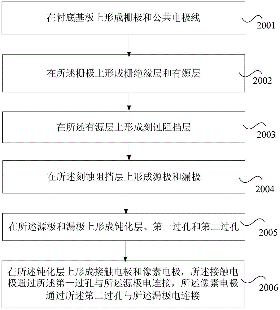
[0033] image 3 It is a flow chart of a method for manufacturing a thin film transistor provided in Embodiment 1 of the present invention. Such as image 3 As shown, the preparation method of the thin film transistor comprises:
[0034] Step 3001, forming a gate in the display area, and forming a first gate metal in the connection area.
[0035] Figure 4 It is a schematic diagram of forming the first source-drain metal, gate and gate insulating layer in the first embodiment. Such as Figure 4 As shown, a gate metal film is formed on the substrate, and the thickness of the gate me...
Embodiment 2
[0054] As an embodiment of the present invention, the array substrate provided in Embodiment 1 of the present invention is an array substrate structure in which the gate layer is located on the bottom layer, but the structure of the array substrate in Embodiment 1 of the present invention is also applicable to the array substrate structure in which the gate layer is located on the top layer .
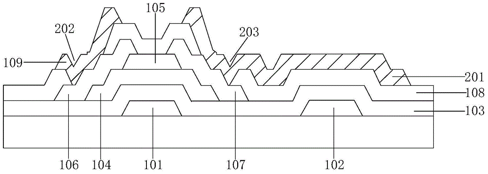
[0055] Figure 13 It is a schematic structural diagram of a thin film transistor provided in Embodiment 2 of the present invention. Such as Figure 13 As shown, the array substrate includes a base substrate, the base substrate includes a display area, and the display area is provided with a gate 101, a gate insulating layer 103, an active layer 104, a source 106, and a drain 107, The source electrode 106 and the drain electrode 107 are completely located above the active layer 104, thereby shortening the process time, improving the production efficiency and reducing the production cos...
Embodiment 3
[0060] Embodiment 3 provides a display device, including any array substrate provided in Embodiment 2. For specific content, refer to the description in Embodiment 2 above, which will not be repeated here. The display device may be any product or component with a display function such as a liquid crystal panel, an electronic paper, an OLED panel, a mobile phone, a tablet computer, a television set, a monitor, a notebook computer, a digital photo frame, a navigator, and the like.
[0061] In the display device provided in the third embodiment, the active layer, the source electrode and the drain electrode are formed through a patterning process, and the source electrode and the drain electrode are arranged above the active layer so as not to affect the quality of the thin film transistor. The use frequency of the mask plate is reduced under the premise, and compared with the prior art, the number of patterning processes is further reduced, the production process is simplified, t...
PUM
| Property | Measurement | Unit |
|---|---|---|
| thickness | aaaaa | aaaaa |
| thickness | aaaaa | aaaaa |
| thickness | aaaaa | aaaaa |
Abstract
Description
Claims
Application Information
 - Generate Ideas
- Intellectual Property
- Life Sciences
- Materials
- Tech Scout
- Unparalleled Data Quality
- Higher Quality Content
- 60% Fewer Hallucinations
Browse by: Latest US Patents, China's latest patents, Technical Efficacy Thesaurus, Application Domain, Technology Topic, Popular Technical Reports.
© 2025 PatSnap. All rights reserved.Legal|Privacy policy|Modern Slavery Act Transparency Statement|Sitemap|About US| Contact US: help@patsnap.com