High-temperature-resistant mylar sheet and preparation method thereof as well as method for protecting wafer in wafer thinning process

A high-temperature-resistant, wafer-based technology, applied in chemical instruments and methods, film/sheet adhesives, semiconductor/solid-state device manufacturing, etc., can solve the problems of high wafer damage rate, poor protection effect, and affecting chip performance, etc. problems, to achieve the effect of good electrical properties, good cushioning, and excellent creep resistance

Active Publication Date: 2015-03-11
马鞍山太时芯光科技有限公司
View PDF5 Cites 3 Cited by
  • Summary
  • Abstract
  • Description
  • Claims
  • Application Information

AI Technical Summary

Problems solved by technology

[0005] Aiming at the problems that the wafer damage rate in the existing chip thinning process is high and the existing chip protection method will affect the performance of the chip and the protection effect is poor, the invention provides a high temperature resistant mylar sheet and its preparation method and chip wafer thinning method. Ways to Protect Wafers in Thin Processes

Method used


Image

  • High-temperature-resistant mylar sheet and preparation method thereof as well as method for protecting wafer in wafer thinning process
  • High-temperature-resistant mylar sheet and preparation method thereof as well as method for protecting wafer in wafer thinning process
  • High-temperature-resistant mylar sheet and preparation method thereof as well as method for protecting wafer in wafer thinning process

Examples


Embodiment 1

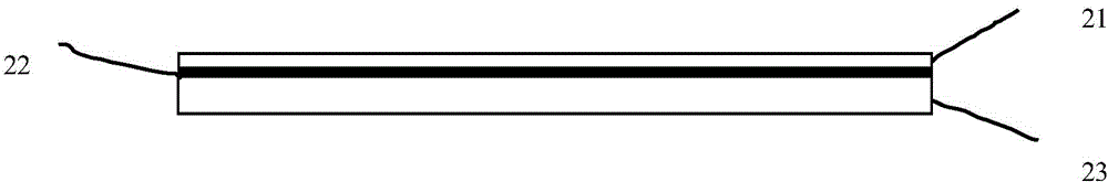
[0046] A high temperature resistant mylar sheet, comprising a PET transparent release film 21, an acrylic adhesive 22 and a PET transparent film 23, the acrylic adhesive 22 is located between the PET transparent release film 21 and the PET transparent film 23, and the PET transparent release film 21 The thickness of the PET transparent film 23 is 25 μm, and the thickness of the PET transparent film 23 is 80 μm.

[0047] In order to obtain above-mentioned high temperature resistant mylar sheet, a kind of preparation method of high temperature resistant mylar sheet, its steps are:

[0048] (a) Prepare the required dimethyl terephthalate, ethylene glycol, biaxial stretching film making machine, glue coating machine, acrylic adhesive, PET transparent release film for the preparation of high temperature resistant mylar sheets;

[0049] (b) In the 10,000-level clean environment production workshop (the air humidity in the workshop is 70%), polyethylene terephthalate is obtained thro...

Embodiment 2

[0066] Same as Example 1, the difference is: in the high temperature resistant mylar sheet, the thickness of the PET transparent release film 21 is 22 μm, and the thickness of the PET transparent film 23 is 85 μm;

[0067] A preparation method of high temperature resistant mylar sheet, the steps are the same as in Example 1, the difference is: the air humidity in the workshop in step (b) is 80%; Apply a layer of 4 μm thick acrylic adhesive evenly on the PET transparent film obtained in (b); in step (d), when the temperature drops to 30° C., stick the PET transparent release film on the acrylic adhesive.

[0068] The high temperature resistant mylar sheet prepared in this example is tested, and its performance is shown in Table 2: the adhesive force is 28g / 30mm, it is very firm and stable in adhesion to the ceramic disc, and has a long service life, and its total light transmittance is 83%, it is convenient to observe whether there are air bubbles between the high temperature r...

Embodiment 3

[0074] Same as Example 1, the difference is: in the high temperature resistant mylar sheet, the thickness of the PET transparent release film 21 is 27 μm, and the thickness of the PET transparent film 23 is 75 μm;

[0075] A preparation method of high temperature resistant mylar sheet, the steps are the same as in Example 1, the difference is: the air humidity in the workshop in step (b) is 75%; Apply a layer of 6 μm thick acrylic adhesive evenly on the PET transparent film obtained in (b); in step (d), when the temperature drops to 30° C., stick the PET transparent release film on the acrylic adhesive.

[0076] The high temperature resistant mylar sheet prepared in this example is tested, and its performance is shown in Table 3: the adhesive force is 22g / 30mm, it is very firm and stable in adhesion to the ceramic disc, and has a long service life, and its total light transmittance is 91%, it is convenient to observe whether there are air bubbles between the high temperature r...


PUM

PropertyMeasurementUnit
thicknessaaaaaaaaaa
thicknessaaaaaaaaaa
thicknessaaaaaaaaaa

Abstract

The invention discloses a high-temperature-resistant mylar sheet and a preparation method thereof as well as a method for protecting a wafer in a wafer thinning process, and belongs to the field of semiconductor silicon device and integrated circuit manufacture. The high-temperature-resistant mylar sheet comprises a PET (polyethylene terephthalate) transparent release film, an acrylic acid type adhesive and a PET transparent film. In the wafer thinning process, the high-temperature-resistant mylar sheet is adhered to a ceramic plate and further is coated with low-temperature wax; and during wafer thinning, the high-temperature-resistant mylar sheet buffers hard-to-hard contact between a substrate and the ceramic plate and protects smoothness and flatness of the surface of the ceramic plate. The fragmenting rate during wafer thinning can be reduced, the chip productivity is improved, besides, wear of the ceramic plate can be reduced, the service life of the ceramic plate is prolonged, the production cost is reduced, the economic benefit is high, and the high-temperature-resistant mylar sheet is suitable for industrial application.

Description

technical field [0001] The invention belongs to the field of semiconductor silicon device and integrated circuit manufacturing, and more specifically relates to a high-temperature-resistant mylar sheet, a preparation method thereof, and a method for protecting a wafer in a wafer thinning process. Background technique [0002] A semiconductor refers to a material whose conductivity is between that of a conductor and an insulator at room temperature. It is widely used in radios, televisions, and temperature measurement. Diodes are a semiconductor material. The manufacturing process of semiconductor silicon devices and integrated circuit dies must have a wafer thinning process for finished chips. The purpose of thinning is to enable the wafer to dissipate heat better during use and prolong its service life. The thinning of semiconductor chips and other devices is the thinning of the entire wafer. Usually, the excess thickness is subtracted from the back of the wafer by grinding...

Claims


Application Information

Patent Timeline
Patent Type & Authority Applications(China)
IPC IPC(8): C09J7/02B32B7/06B32B7/12B32B27/06B32B27/36H01L21/02H01L21/683
Inventor 靖明亮董成李有群廉鹏
Owner 马鞍山太时芯光科技有限公司
Why Eureka
Try Eureka