A kind of vertical LED structure and manufacturing method thereof

A technology of LED structure and manufacturing method, applied in electrical components, circuits, semiconductor devices, etc., can solve the problems of increasing the production cost of LED chips, increasing the production cost, etc., to solve the problem of brightness improvement, solve the problem of heat dissipation, and reduce the production cost. Effect

Active Publication Date: 2017-11-24
HANGZHOU SILAN AZURE
View PDF3 Cites 0 Cited by
  • Summary
  • Abstract
  • Description
  • Claims
  • Application Information

AI Technical Summary

Problems solved by technology

However, like high-voltage chips, vertical structure LEDs also need to form isolation grooves, and most of the existing flip-chip vertical LED structures use precious metal silver with the highest reflectivity in nature as the specular reflection layer, which greatly increases the production cost of LEDs. Not only that, silver is a metal that is very easy to oxidize, sulfide and migrate, so in order to suppress the oxidation, sulfide and migration of silver, other materials and processes must be used to make passivation layers, barrier layers, protective layers, etc., so this is another Increased the production cost of LED chips at one time

Method used


Image

  • A kind of vertical LED structure and manufacturing method thereof
  • A kind of vertical LED structure and manufacturing method thereof
  • A kind of vertical LED structure and manufacturing method thereof

Examples


Embodiment Construction

[0042]Various exemplary embodiments of the present invention will now be described in detail with reference to the accompanying drawings.

[0043] Such as Figure 15 As shown, the vertical LED structure manufacturing method of the present invention comprises the following steps:

[0044] S1: providing a substrate;

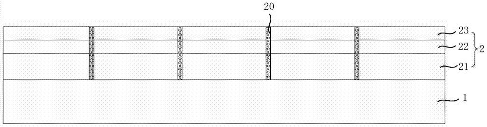
[0045] S2: forming a light-emitting semiconductor layer on the substrate, and forming several high-resistance ion implantation layers at predetermined positions of the light-emitting semiconductor layer through an ion implantation process, and the several high-resistance ion implantation layers divide the light-emitting semiconductor layer Form a number of independent light-emitting semiconductor layers that are insulated and separated, and each independent light-emitting semiconductor layer includes an N-type semiconductor layer, an active layer, and a P-type semiconductor layer stacked in sequence;

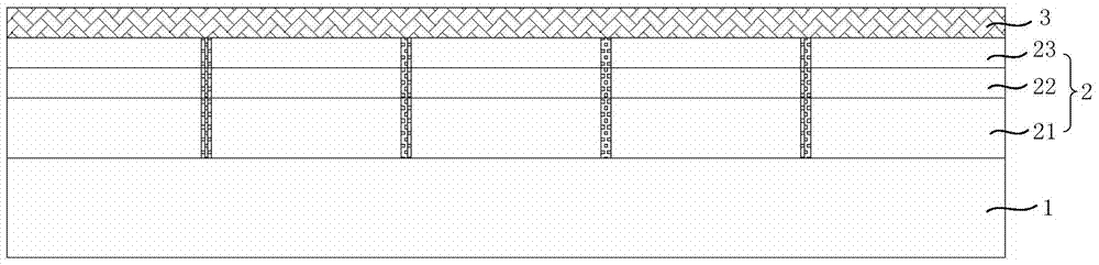
[0046] S3: forming an independent contact layer on the P-type...


PUM


Abstract

The invention provides a vertical LED structure and a manufacturing method thereof. The manufacturing method comprises the following steps: cutting an epitaxial layer into a plurality of insulated and separated independent light emitting semiconductor layers through the ion implantation technique to replace the traditional complex processes of firstly manufacturing an isolation groove and then filling an insulated material, forming an independent contact layer on each independent light emitting semiconductor layer, then forming a net-shaped-structure DBR reflection layer on each independent contact layer to replace a silver specular reflection layer, and then forming an independent metal function layer on the net-shaped-structure DBR reflection layer. According to the invention, the net-shaped-structure DBR reflection layer is arranged on the independent contact layer to replace the silver specular reflection layer, and the cheap independent metal function layer is arranged on the net-shaped-structure DBR reflection layer, the production cost of an LED is reduced while the problems of brightness improvement and heat dissipation are solved, and the manufacturing method is suitable for large-scale commercialized production.

Description

technical field [0001] The invention belongs to the field of semiconductor photoelectric chip manufacturing, and in particular relates to a vertical LED structure and a manufacturing method thereof. Background technique [0002] Since its commercialization in the early 1990s, after more than 20 years of development, GaN-based LEDs have been widely used in indoor and outdoor display screens, lighting sources for projection displays, backlight sources, landscape lighting, advertising, traffic instructions, etc. Field, and known as the most competitive new generation of solid-state light source in the 21st century. However, for the semiconductor light-emitting device LED, in order to replace the traditional light source and enter the high-end lighting field, three problems must be solved at the same time: one is to solve the problem of luminous brightness improvement, the other is to solve the heat dissipation problem, and the third is to solve the production cost reduction. q...

Claims


Application Information

Patent Timeline
Patent Type & Authority Patents(China)
IPC IPC(8): H01L33/02H01L33/10H01L33/00
CPCH01L33/005H01L33/02H01L33/10H01L33/20H01L2933/0008
Inventor 张昊翔丁海生李东昇江忠永
Owner HANGZHOU SILAN AZURE
Why Eureka
Try Eureka