Through-silicon via and forming method thereof

A technology of through-silicon via and silicon germanium, which is applied in electrical components, electrical solid-state devices, circuits, etc., can solve the problems of holes in conductive pillars, unsatisfactory effects, and decreased electrical conductivity, so as to save costs, save process costs, and reduce The effect of energy consumption

Active Publication Date: 2015-03-18
SEMICON MFG INT (SHANGHAI) CORP +1
View PDF5 Cites 2 Cited by
  • Summary
  • Abstract
  • Description
  • Claims
  • Application Information

AI Technical Summary

Problems solved by technology

Once the hole 13 appears inside the conductive column 12, the resistance of the TSV will increase, the electrical conductivity will decrease, the electrical connection performance will be poor, and even electromigration and stress migration will occur, which will lead to a decrease in the reliability of the TSV.
[0006] Although it has been proposed to increase the opening o

Method used


Image

  • Through-silicon via and forming method thereof
  • Through-silicon via and forming method thereof
  • Through-silicon via and forming method thereof

Examples


Embodiment Construction

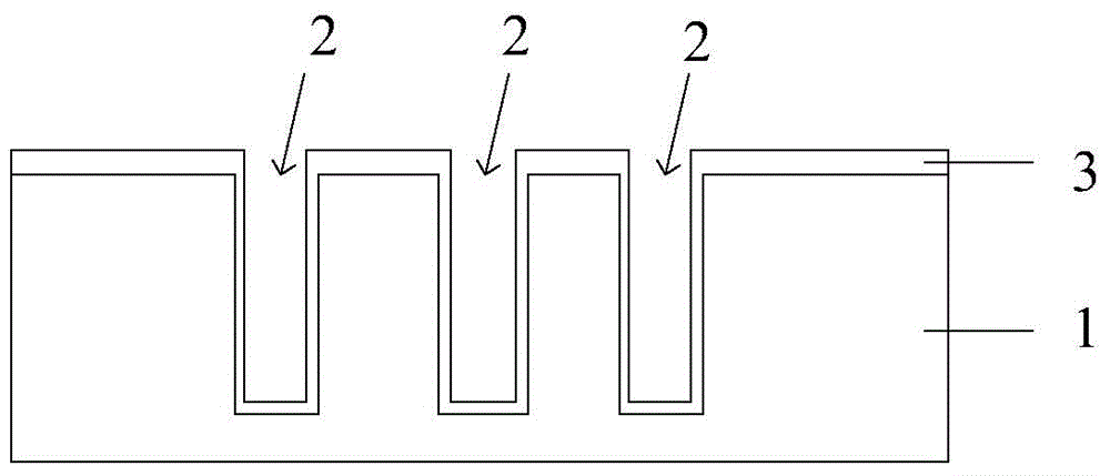
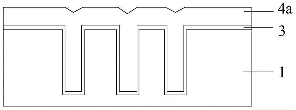
[0027] In the existing method, copper or tungsten is usually used for filling in the process of forming the through-silicon vias.

[0028] When copper filling is used, electroplating copper is usually used. With the decrease of the width of the through-hole and the increase of the depth of the through-hole in the through-silicon via, the bottom area of ​​the through-hole decreases, and the bottom of the through-hole is concave, which leads to the increase of the resistance at the bottom of the through-hole, and even the appearance of a through-hole The bottom resistance is greater than the side resistance of the through hole. Therefore, during the copper electroplating process, the copper deposition rate on the side of the through hole is greater than the copper deposition rate at the bottom of the through hole, resulting in holes in the formed copper pillars.

[0029] When tungsten is used for filling, chemical vapor deposition of metal organic compounds is usually adopted, a...


PUM

PropertyMeasurementUnit
Depthaaaaaaaaaa

Abstract

Provided are a through-silicon via and a forming method thereof. The forming method of the through-silicon via comprises the following steps: a semiconductor substrate is provided, wherein the semiconductor substrate has a through via, and the surface of the through via is coated with an insulating layer; and the through via is filled with silicon germanium. By making use of good filling capacity of silicon germanium and filling the through via with silicon germanium, a formed conductive column has no hole inside. Therefore, a through-silicon via formed by the method has stable performance and high reliability.

Description

technical field [0001] The invention relates to the field of semiconductor technology, in particular to a through-silicon hole and a forming method thereof. Background technique [0002] With the continuous development of semiconductor technology, the feature size of semiconductor devices has become very small. It is becoming more and more difficult to increase the number of semiconductor devices in a two-dimensional packaging structure. Therefore, three-dimensional packaging has become a method that can effectively improve chip integration. degree method. Current three-dimensional packaging includes die stacking based on wire bonding, package stacking and three-dimensional stacking based on through silicon vias (Through Silicon Via, TSV). [0003] The three-dimensional stacking technology based on through-silicon vias has the following three advantages: (1) high-density integration; (2) greatly shortening the length of electrical interconnections, which can well solve the ...

Claims


Application Information

Patent Timeline
IPC IPC(8): H01L23/528H01L21/768
Inventor 郭亮良黄河骆凯玲
Owner SEMICON MFG INT (SHANGHAI) CORP
Why Eureka
Try Eureka