Superhigh-definition CMOS image sensor pixel circuit and control method thereof

An image sensor and pixel circuit technology, applied in the field of image sensing, can solve the problems of increasing the size of the camera and increasing the cost, and achieve the effects of reducing fixed image noise, high absorption rate, and low fixed noise

Inactive Publication Date: 2015-03-18
BEIJING INST OF COMP TECH & APPL +1
View PDF6 Cites 3 Cited by
  • Summary
  • Abstract
  • Description
  • Claims
  • Application Information

AI Technical Summary

Problems solved by technology

Disadvantages: increase the size of the camera and increase the cost
Of course, when the automatic gain function (AGC) amplifies the signal, it also amplifies the noise, but the improvement in illumination is still very obvious

Method used


Image

  • Superhigh-definition CMOS image sensor pixel circuit and control method thereof
  • Superhigh-definition CMOS image sensor pixel circuit and control method thereof
  • Superhigh-definition CMOS image sensor pixel circuit and control method thereof

Examples


Embodiment Construction

[0050] The technical solution of the present invention will be described in detail below in conjunction with the accompanying drawings and specific embodiments to further understand the purpose, solution and effect of the present invention, but it is not intended to limit the scope of protection of the appended claims of the present invention.

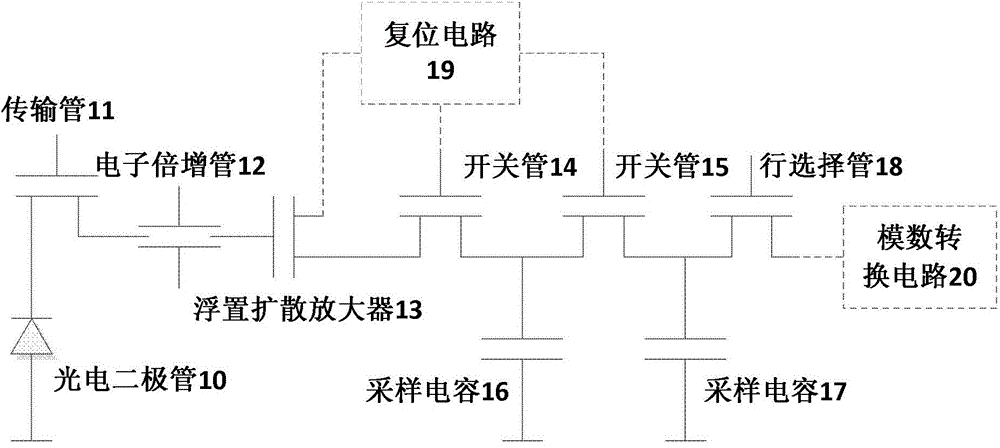
[0051] Such as figure 1 Shown is a pixel circuit diagram of an ultra-high-definition CMOS image sensor capable of recognizing ultra-low illumination visible light of the present invention.

[0052] exist figure 1 Among them, the pixel circuit consists of a photodiode 10, a transmission tube 11, a single-channel electron multiplier 12, a floating diffusion amplifier 13, a first switching tube 14, a second switching tube 15, a first sampling capacitor 16, a second sampling capacitor 17, Row selection tube 18, reset circuit 19, and analog-to-digital conversion circuit 20 are composed. The first switching tube 14 , the second switching t...


PUM


Abstract

The invention discloses a superhigh-definition CMOS image sensor pixel circuit and a control method thereof. The circuit comprises a photosensitive element, a transmission pipe, a single-channel electron multiplier, a floating diffusion amplifier, a correlation double-sampling circuit, a row selection tube, a reset circuit and an analog-to-digital conversion circuit. The photosensitive element generates electrons, the transmission tube is closed, the correlation double-sampling circuit samples noise signals generated by the single-channel electron multiplier and the floating diffusion amplifier to obtain first sampling signals, and the row selection tube transmits the first sampling signals to the analog-to-digital conversion circuit; the transmission tube is opened, the floating diffusion amplifier converts the electrons after the multiplication of the single-channel electron multiplier into voltage signals, and the correlation double-sampling circuit samples the voltage signals to obtain second sampling signals; and the analog-to-digital conversion circuit performs correlation double-sampling processing according to the first sampling signals and the second sampling signals to obtain image signals. According to the invention, visible light with ultra-low illumination can be identified through low-solid-state noise.

Description

technical field [0001] The invention relates to the field of image sensing, in particular to an improvement of a pixel structure and a circuit of a CMOS image sensor for recognizing ultra-low illumination visible light and a circuit control method for ultra-high-definition requirements. Background technique [0002] In recent years, with the expansion of the scope and connotation of monitoring applications, especially the wide application of full HD and ultra-high It is difficult to monitor under low-illuminance conditions such as night monitoring of roads and residential areas, or even in ultra-low-illuminance environments such as underground roadways and tunnels. The production of the ultra-low illumination camera is a product produced to solve the application of this special ultra-low illumination environment. Its main advantage is that in an environment with very low illumination, it can increase the illumination as much as possible to capture the monitored object. . ...

Claims


Application Information

Patent Timeline
Patent Type & Authority Applications(China)
IPC IPC(8): H04N5/374
Inventor 钟松延苏威积裴彦杰林秀春肖鹏张力黄敏君董一伯杜丽邓超刘攀孟飞董博赵薇牛坤张健刘雨睿王东东张春杰黄传鹤
Owner BEIJING INST OF COMP TECH & APPL
Why Eureka
Try Eureka