

wavy mos 2 Nanosheet inlaid dandelion tio 2 Nanosphere composite heterojunction semiconductor material and preparation method thereof
A composite heterojunction and dandelion technology, applied in chemical instruments and methods, chemical/physical processes, physical/chemical process catalysts, etc., can solve problems such as inapplicability to large-scale industrial production, complex synthesis processes, and high production costs. Achieve low cost, enhanced catalytic performance, and high reproducibility
- Summary
- Abstract
- Description
- Claims
- Application Information
AI Technical Summary
Problems solved by technology
Method used
Image

Examples
Embodiment 1
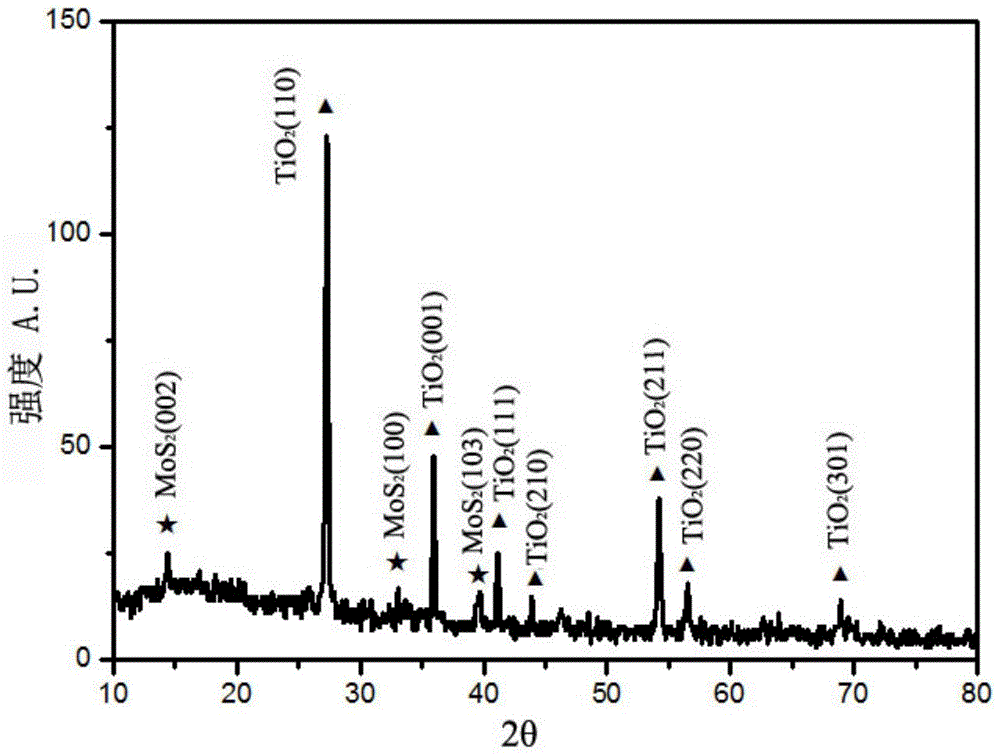
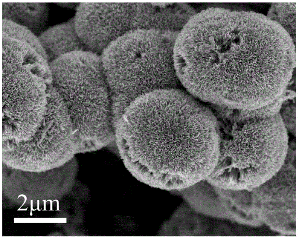
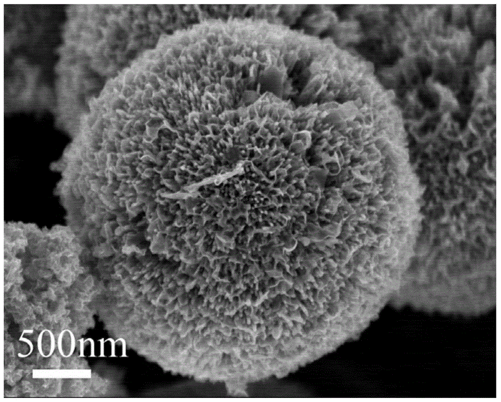
[0034] Example 1 Preparation of wavy MoS 2 Nanosheet mosaic dandelion TiO 2 Nanosphere Composite Heterojunction Semiconductor Materials
[0035] The specific steps of preparation are as follows:
[0036] (1) Add 2 mL of 35% hydrochloric acid and 4 mL of tetrabutyl titanate into a small Erlenmeyer flask and shake and mix. It is found that the reaction generates high temperature. At this time, the Erlenmeyer flask is placed in cold water to cool rapidly. After cooling completely, Slowly drop the mixed solution into a beaker containing 20mL oleic acid while stirring.
[0037] (2) After stirring for more than 15 minutes, it will be found that the color of the solution gradually changes from egg yellow to orange and remains unchanged. At this time, the mixed solution is added to a 50mL reaction kettle, sealed, and then heated in a vacuum oven at 180°C for 4 Hours, the reaction was completed and cooled to room temperature.
[0038] (3) Wash the white precipitate at the bottom of...
Embodiment 2
[0045] Example 2 Wave MoS of the present invention 2 Nanosheet mosaic dandelion TiO 2 Photocatalytic Performance Test of Nanosphere Composite Heterojunction Semiconductor Materials
[0046] The wavy MoS of the present invention prepared in the above-mentioned Example 1 2 Nanosheet mosaic dandelion TiO 2 Nanosphere composite heterojunction semiconductor materials, due to their large specific surface area and the formation of p-n junctions at the junction, make them comparable to pure TiO 2 The photocatalytic performance of dandelion nanospheres has been significantly improved. Wave MoS of the present invention 2 Nanosheet mosaic dandelion TiO 2 Nanosphere Composite Heterojunction Semiconductor Materials and TiO 2 Photocatalytic performance test of dandelion nanospheres, including specific steps:
[0047] (1) Take two identical brown jars, put 100ml of methylene blue solution in each bottle, the solution concentration is 10mg L -1 .
[0048] (2) Take the wave MoS of the...
PUM
| Property | Measurement | Unit |
|---|---|---|
| diameter | aaaaa | aaaaa |
Abstract
Description
Claims
Application Information