Laser scribing method reducing chip physical stress damage

A laser scribing and physical stress technology, applied in laser welding equipment, electrical components, circuits, etc., can solve the problems of inability to mass-produce Flash products, hinder the application and promotion of laser scribing, damage Flash products, etc., and achieve yield Improve, reduce impact, reduce the effect of damage rate

Active Publication Date: 2015-03-25
SHANGHAI HUAHONG INTEGRATED CIRCUIT
View PDF6 Cites 4 Cited by
  • Summary
  • Abstract
  • Description
  • Claims
  • Application Information

AI Technical Summary

Problems solved by technology

[0002] Traditional diamond knife scribing cannot perform scribing on Flash (flash memory) products with scribing lines less than 20 μm
[0003] The laser scribing process method has been widely used and promoted in the fields of LED (light-emitting diode) and RFID (radio frequency identification); however, in the field of Flash products with higher integration, smaller

Method used


Image

  • Laser scribing method reducing chip physical stress damage

Examples


Embodiment Construction

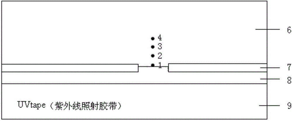
[0010] Referring to the accompanying drawings, the laser scribing method that reduces the chip damage by physical stress is:

[0011] Put the thinned wafer with the back of the wafer (6 indicates the wafer monocrystalline silicon substrate) facing up and the front (7 indicates the effective layer of the chip circuit on the front of the wafer) facing down, and pass through the UV tape (ultraviolet irradiation tape). The covered UV glue (shadowless glue) (8 indicates the UV adhesive layer covered by UV tape) is applied on the UV film (ultraviolet film) [9 indicates the PC (polycarbonate) film layer of UVtape]; the back of the wafer faces The laser source is incident from the back of the wafer to perform scribing, and the first laser scan focuses on the front surface of the wafer scribing lane. 1 in the figure indicates the position of the focus point of the first laser scanning in the scribing track, and 2, 3, 4, etc. respectively indicate the longitudinal position and order of ...


PUM

PropertyMeasurementUnit
Wavelengthaaaaaaaaaa

Abstract

The invention discloses a laser scribing method reducing chip physical stress damage. According to the technical scheme, the method includes emitting laser to the back of a wafer, and focusing the front surfaces of wafer scribing channels through primary laser scanning; selecting the laser source energy with the set strength, allowing the covalent bonds between the surface crystals of the wafer scribing channels to break completely to obtain an amorphous layer so as to reduce the transmission capability of mechanical stress; performing multiple times of laser scanning in the same scribing channel, and allowing the scanning laser focusing depth to decrease sequentially; allowing the distances between the scanning laser focusing points to be smaller than or equal to the effective bond breaking area radius of the adopted laser source. By the aid of the method, the damage on Flash products with the scribing channels which are smaller than 20 micrometers by laser scribing can be reduced greatly, and the laser scribing can be applied to the Flash products with the scribing channels which are smaller than 20 micrometers in batches. The method is adaptive to the Flash products with the scribing channels which are smaller than 20 micrometers.

Description

technical field [0001] The invention relates to the field of hidden laser scribing of wafers in integrated circuit manufacturing, in particular to a laser scribing method capable of reducing physical stress damage to chips in a laser scribing process method for wafers with a scribing track width less than 20 μm. Background technique [0002] Traditional diamond scribing cannot perform scribing on Flash (flash memory) products with scribing lines smaller than 20 μm. [0003] The laser scribing process method has been widely used and promoted in the fields of LED (light-emitting diode) and RFID (radio frequency identification); however, in the field of Flash products with higher integration, smaller feature size, and lower cost requirements, due to laser scribing Micro-damages caused by thermal stress and physical stress caused by chips can damage Flash products, resulting in a loss of yield that cannot be ignored, and cannot be mass-produced and applied to Flash products, whi...

Claims


Application Information

Patent Timeline
IPC IPC(8): B23K26/38H01L21/78
CPCB23K26/53B23K2101/40H01L21/78
Inventor 王光振
Owner SHANGHAI HUAHONG INTEGRATED CIRCUIT
Why Eureka
Try Eureka