All-side-pin-free flat semiconductor device packaging structure and method
A four-sided no-lead, device packaging technology, which is applied in semiconductor devices, semiconductor/solid-state device manufacturing, semiconductor/solid-state device components, etc., can solve the problems of low production efficiency, extra heat of wires, limited current carrying capacity of semiconductor devices, and poor reliability and other issues, to achieve the effect of improving production efficiency, saving bridge frame placement machines, and low parasitic voltage
- Summary
- Abstract
- Description
- Claims
- Application Information
AI Technical Summary
Problems solved by technology
Method used
Image
Examples
Embodiment 1
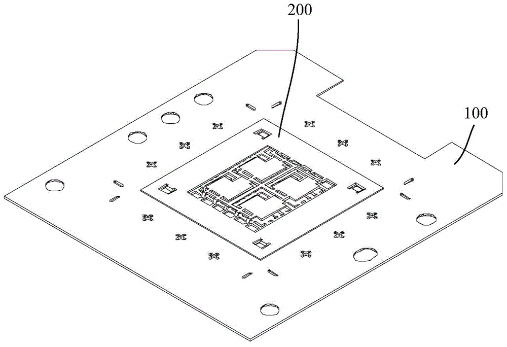
[0053] figure 1 It is the overall structure diagram of the four-sided leadless flat semiconductor device package structure provided by the first embodiment of the present invention. Such as figure 1 As shown, the package structure includes:
[0054] Lead frame 100 and bridge frame 200.
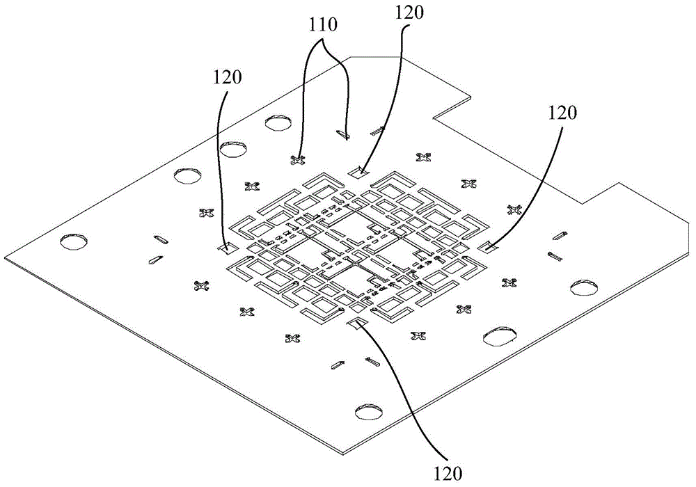
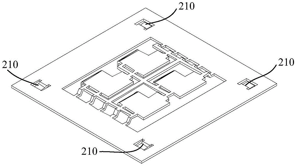
[0055] figure 2 It is the lead frame structure diagram of the four-sided leadless flat semiconductor device package structure provided by the first embodiment of the present invention. Such as figure 2 As shown, the edge of the lead frame is provided with a plurality of cutting positioning marks 110. When the semiconductor device is packaged with this packaging structure, the bridge frame is stacked on the lead frame, and when stacked, the cutting positioning marks on the lead frame are exposed. At least one first positioning bayonet 120 is provided on the lead frame, which is mutually engaged with the second positioning bayonet on the bridge frame when used for packaging, so that the positionin...
Embodiment 2
[0078] Image 6 It is a flowchart of a four-sided leadless flat semiconductor device packaging method provided in the second embodiment of the present invention. Such as Image 6 As shown, the packaging method includes:
[0079] Step 601: Dicing the wafer to obtain multiple chips.
[0080] In this step, the wafer with multiple chips is cut to obtain multiple chips.
[0081] Step 602: Provide a lead frame. A plurality of cutting positioning marks are provided on the edge of the lead frame, and the cutting positioning marks divide the lead frame into multiple rows and multiple columns of connected lead frame units.
[0082] In this step, the lead frame structure and the lead frame unit structure are as described in the first embodiment.
[0083] Step 603: Prepare conductive bonding material on the first chip holder, the first chip gate pin and the second chip holder.
[0084] In this step, the conductive bonding material is coated on the first chip holder, the first chip gate pin and th...
PUM
 Abstract
Description
Claims
Application Information


