Integrated Circuit Reliability Analysis Test Structure and Test Method

A technology for analysis and testing of integrated circuits, applied in the field of reliability analysis and testing structures of integrated circuits, can solve problems such as structures that do not deliberately and accurately evaluate the reliability of side trench isolation, and affect the electrical characteristics of devices, so as to achieve accurate evaluation of reliability Effect

Active Publication Date: 2017-10-27
SEMICON MFG INT (SHANGHAI) CORP
View PDF3 Cites 0 Cited by
  • Summary
  • Abstract
  • Description
  • Claims
  • Application Information

AI Technical Summary

Problems solved by technology

The depth of the side ditch will affect the characteristics of the semiconductor (MOS) device in its vicinity. Due to the formation of the side ditch, the polysilicon filled in this part will form an inversion layer on the side wall of the active region, resulting in a parasitic current path, which in turn affects Electrical Characteristics of the Device
[0004] However, in the prior art, there is no structure for deliberately and accurately evaluating the impact of side trenches on the reliability of shallow trench isolation

Method used


Image

  • Integrated Circuit Reliability Analysis Test Structure and Test Method
  • Integrated Circuit Reliability Analysis Test Structure and Test Method
  • Integrated Circuit Reliability Analysis Test Structure and Test Method

Examples


no. 1 example

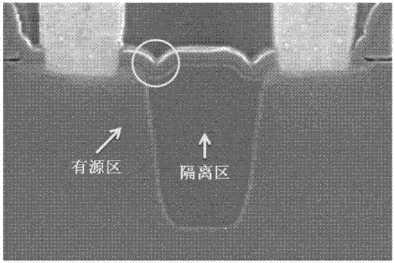
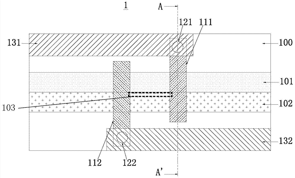
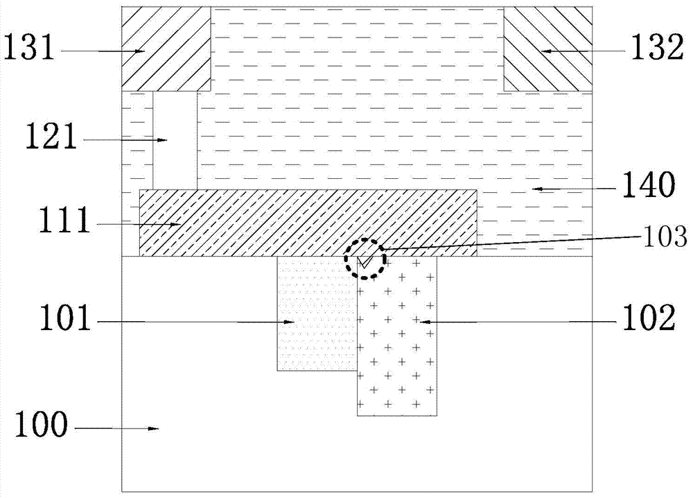
[0054] In the first embodiment, the test structure 1 includes a first gate structure and a second gate structure. Please refer to Figure 2-Figure 3 The reliability analysis and test structure of the integrated circuit is specifically described, where: figure 2 Is a top view of an integrated circuit reliability analysis test structure in an embodiment of the present invention, image 3 for figure 2 In the cross-sectional view along the cut line A-A', the dielectric 140 is common technical knowledge known in the art, so in order to clearly illustrate the structure of this embodiment, figure 2 The dielectric 140 is omitted in the image 3 Clearly shown in.

[0055] Such as figure 2 As shown, the substrate 100 includes an active region 101 and an isolation region 102, wherein the shape, size, number, and arrangement of the active region 101 and the isolation region 102 are not specifically limited, depending on the circuit design (Design) For example, in this embodiment, the acti...

no. 2 example

[0064] Please refer to Image 6 , Image 6 Is a top view of an integrated circuit reliability analysis test structure in another embodiment of the present invention, Figure 7 for Image 6 A cross-sectional view along the section line B-B'. In the figure, the same reference numerals indicate equivalent Figure 1-Figure 5 The label in. The second embodiment is based on the first embodiment. The difference is that the reliability analysis test structure 2 of the integrated circuit includes two first gate structures 111 and two second gate structures 112, The first gate structure 111 and the second gate structure 112 are arranged alternately.

[0065] Preferably, the first metal line structure 131 and the second metal line structure 132 are both a metal connection line, the first metal line structure 131 is perpendicular to the first gate structure 111, and the second metal line The structure 132 is perpendicular to the second gate structure 112, and the first metal line structure ...


PUM


Abstract

The invention discloses a reliability analysis test structure of an integrated circuit. The test structure comprises: a substrate, a first gate structure, a first metal line structure, a second gate structure, a second metal line structure and a dielectric. The invention also discloses a testing method of the testing structure, including: actually forming a structure to be tested according to the testing structure; and testing the electrical reliability between the first metal wire structure and the second metal wire structure. In the test structure of the present invention, the first gate structure and the second gate structure are arranged in parallel, and straddle the active region and the isolation region, so that the through hole on the active region and the adjacent The reliability of the dielectric between the gates.

Description

Technical field [0001] The invention relates to the field of reliability (Reliability) in the semiconductor manufacturing industry, in particular to a reliability analysis test structure and a test method of an integrated circuit. Background technique [0002] As the feature size of semiconductor devices continues to shrink, the isolation area between the devices will also be reduced accordingly. The traditionally used Localized Oxidation of Silicon (LOCOS) technology uses a field oxidation process, so the depth of the oxide film and the bird's beak effect on the active area at the edge of the isolation area due to oxidation limit this A further application of technology. Shallow Trench Isolation (STI) technology is the standard isolation technology for deep submicron processes. At present, 0.18μm technology has become the mainstream technology for large-scale products. STI uses silicon nitride as a protective layer to etch trenches in a silicon single crystal substrate throug...

Claims


Application Information

Patent Timeline
Patent Type & Authority Patents(China)
IPC IPC(8): H01L23/544G01R31/26G01R31/28
Inventor 钟怡
Owner SEMICON MFG INT (SHANGHAI) CORP
Why Eureka
Try Eureka