Patterned opto-electrical substrate and method for manufacturing the same

一种光电基板、制作方法的技术,应用在电路、电气元件、半导体/固态器件制造等方向,能够解决发光效率的程度限制、降低差排密度程度等问题

Active Publication Date: 2015-03-25
KINIK
View PDF4 Cites 15 Cited by
  • Summary
  • Abstract
  • Description
  • Claims
  • Application Information

AI Technical Summary

Problems solved by technology

[0007] However, in the above-mentioned inventive diodes, a nanoscale porous photonic crystal structure or micron-scale protruding particles are mainly formed on the substrate alone to improve the luminous efficiency of the light-emitting diode. The degree of dislocation density or the degree of improving luminous efficiency still has its intrinsic limit

Method used


Image

  • Patterned opto-electrical substrate and method for manufacturing the same
  • Patterned opto-electrical substrate and method for manufacturing the same
  • Patterned opto-electrical substrate and method for manufacturing the same

Examples


Embodiment 1

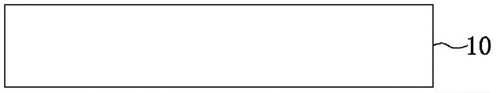
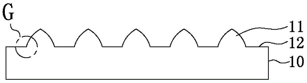
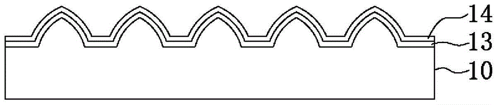
[0047] Please refer to Figures 1A to 1H , is a schematic diagram of the preparation process of the patterned optoelectronic substrate according to Example 1 of the present invention. First, please refer to Figure 1A and Figure 1B , provide a substrate 10, the substrate 10 is a sapphire substrate or a silicon substrate with a planar surface, and a first patterned structure 11 and a spacer region 12 are formed on the surface of the substrate 10 by the first etching process; wherein, in the first etching During the processing, a first photoresist layer (not shown) is provided on a part of the surface of the substrate 10, so that the first etching process selectively removes part of the substrate 10 to form micron-scale protrusions with a conical shape. The first patterned structure 11 of the structure and the spacer region 12 of the planar structure, and the height of the first patterned structure 11 (that is, the micron-scale protrusion structure) is 1.2 microns to 2 microns...

Embodiment 2

[0053] Please refer to figure 2 , is a schematic diagram of the patterned optoelectronic substrate of Example 2 of the present invention. Embodiment 2 is substantially the same as the patterned optoelectronic substrate and its manufacturing process described in Embodiment 1, except that the concave-convex pattern of the first patterned structure is different. Different from Embodiment 1, it is the first patterned structure with a conical micron-scale protrusion structure (please refer to Figure 1B ), in Embodiment 2, a first photoresist layer (not shown) is provided on a part of the surface of the substrate 20, so that the first etching process is to selectively remove part of the substrate 20 to form a cone-shaped The first patterned structure 21 of the micron-scale groove structure and the spacer region 22 of the planar structure; then, according to the manufacturing process of embodiment 1, the first patterned structure 21 contains a plurality of second patterned structu...

Embodiment 3 to Embodiment 5

[0055] Please refer to Figures 3A to 3C , are schematic diagrams of patterned optoelectronic substrates according to Embodiment 3 to Embodiment 5 of the present invention. Embodiment 3 to Embodiment 5 are substantially the same as the patterned optoelectronic substrate described in Embodiment 1 and the manufacturing process thereof, except that the shape of the first patterned structure is different.

[0056] Different from Embodiment 1, it is the first patterned structure with a conical micron-scale protrusion structure (please refer to Figure 1B ), please refer to Figure 3A , in Embodiment 3, a first photoresist layer (not shown) is provided on a part of the surface of the substrate 301, so that the first etching process is to selectively remove part of the substrate 301 to form a triangular cone-shaped The first patterned structure 311 of the micron-scale protruding structure and the spacer region 321 of the planar structure; then, according to the manufacturing proces...


PUM


Abstract

The present invention relates to a patterned opto-electrical substrate, comprising a substrate, the substrate has a first patterned structure, a spacer region and a second patterned structure, wherein the second patterned structure is formed on one or both of the first patterned structure and the spacer region, and the first patterned structure is a micron-scale protruding structure or a micron-scale recessing structure, while the second patterned structure is a submicron-scale recessing structure. The present invention also relates to a method for manufacturing the aforementioned patterned opto-electrical substrate and light emitting diodes having the aforementioned patterned opto-electrical substrate.

Description

technical field [0001] The present invention relates to a patterned optoelectronic substrate and a manufacturing method thereof, in particular to a substrate having a micron-level first pattern structure and a submicron-level second pattern structure, and a light-emitting diode with the substrate. Background technique [0002] The historical development of human lighting has entered the era of solid-state lighting. Brighter luminous brightness, lower price, longer life, higher stability, etc. are the common goals of the solid-state lighting industry. In the lighting market, the brightness requirement of light-emitting diodes is the first priority. Generally speaking, the maximum light output of light-emitting diodes (L max ) is mainly determined by the external quantum efficiency (η ext ) and maximum operating current (I max ) determined by L max =η ext ×I max , where the external quantum efficiency (η ext ) is the internal quantum efficiency (η int ) and light extrac...

Claims


Application Information

Patent Timeline
Patent Type & Authority Applications(China)
IPC IPC(8): H01L33/10H01L33/00
CPCH01L33/22H01L21/0242H01L21/0243H01L33/005H01L33/007H01L33/12H01L33/32
Inventor 柯文政陈卫国洪福益何嘉哲
Owner KINIK
Why Eureka
Try Eureka