A kind of oled device preparation method

A device and primary color technology, applied in the field of OLED device preparation, can solve the problems of reducing the yield of OLED devices, high maintenance costs, and increasing the cost of OLED devices

Active Publication Date: 2018-01-19
TRULY HUIZHOU SMART DISPLAY
View PDF4 Cites 0 Cited by
  • Summary
  • Abstract
  • Description
  • Claims
  • Application Information

AI Technical Summary

Problems solved by technology

Due to the small opening of FINEMASK, repeated contact with the substrate will cause many defects and reduce the yield of OLED devices. In addition, the production and maintenance costs of FINE MASK are high, and a large number of uses will increase the cost of OLED devices.

Method used


Image

  • A kind of oled device preparation method
  • A kind of oled device preparation method
  • A kind of oled device preparation method

Examples


Embodiment Construction

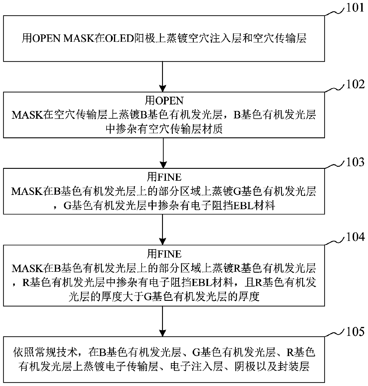
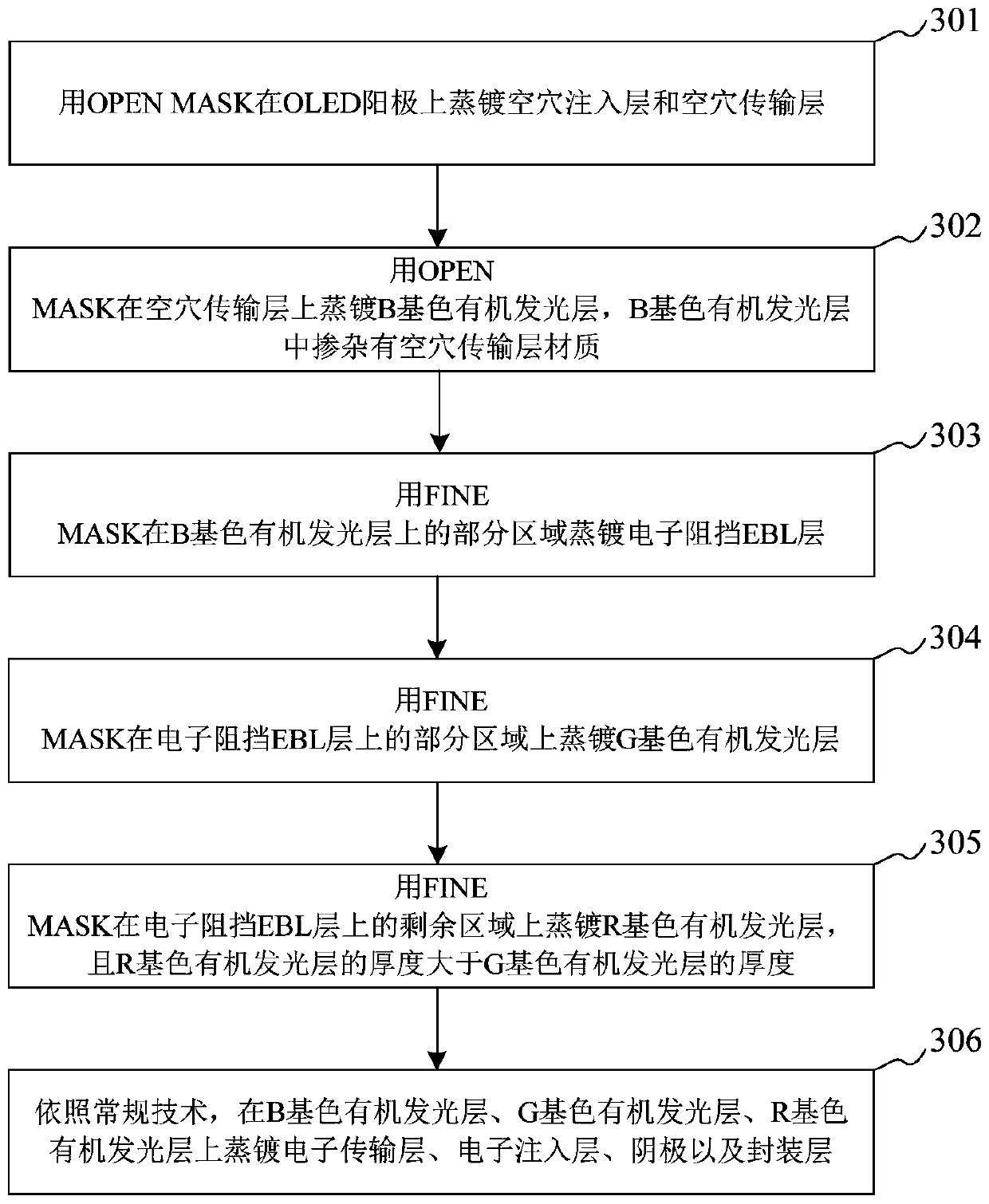
[0028] In order to make the object, technical solution and advantages of the present invention clearer, the present invention will be further described in detail below in conjunction with the accompanying drawings and embodiments. It should be understood that the specific embodiments described here are only used to explain the present invention, not to limit the present invention.

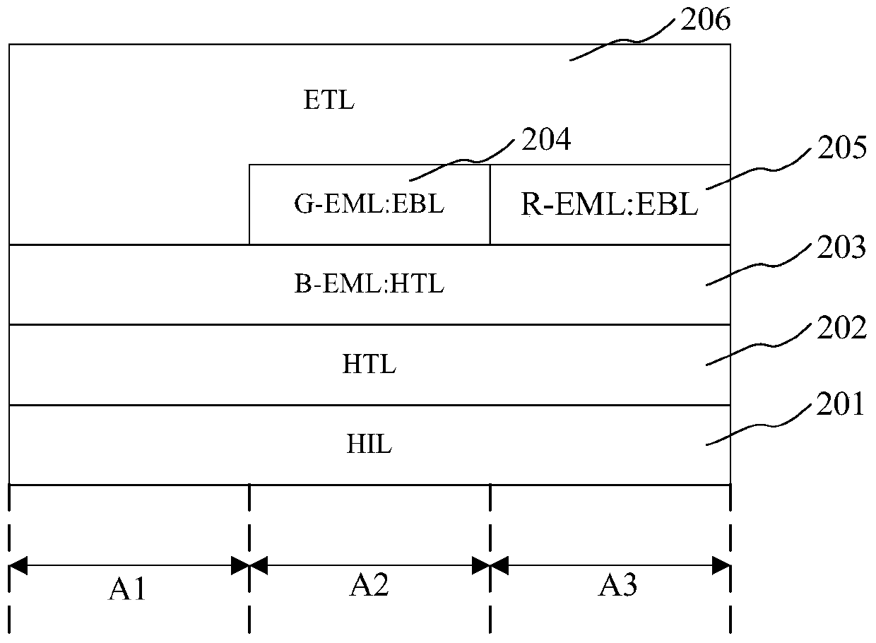
[0029] see figure 1 and figure 2 In one embodiment, a method for preparing an OLED device is provided, the method comprising:

[0030] Step 101, using OPEN MASK to vapor-deposit a hole injection layer and a hole transport layer on the OLED anode.

[0031] Specifically, the OPEN MASK is a mask for vapor deposition, and the opening is relatively large.

[0032] In one embodiment, such as figure 2 As shown, at the OLED anode ( figure 2 Not shown in ), a hole injection layer 201 (HIL, Hole Inject Layer) and a hole transport layer 202 (HTL) are evaporated. The thickness of the hole injection la...


PUM


Abstract

The invention discloses a method for preparing an OLED device, comprising: using OPEN MASK to vapor-deposit a hole injection layer and a hole-transport layer on an OLED anode; , the B primary color organic light emitting layer is doped with a hole transport layer material; FINEMASK is used to vapor-deposit a G primary color organic light emitting layer on a part of the B primary color organic light emitting layer, and the G primary color organic light emitting layer is doped with Doped with electron-blocking EBL materials; use FINE MASK to vapor-deposit an R-base color organic light-emitting layer on a part of the B-base color organic light-emitting layer, and the R-base color organic light-emitting layer is doped with an electron-blocking EBL material, and the The thickness of the R primary color organic light-emitting layer is greater than the thickness of the G primary color organic light-emitting layer; according to conventional techniques, electrons are evaporated on the B primary color organic light-emitting layer, the G primary color organic light-emitting layer, and the R primary color organic light-emitting layer. transport layer, electron injection layer, cathode and encapsulation layer. By applying the technical scheme of the invention, it is possible to avoid using multiple FINEMASK sheets when adjusting the cavity lengths of the three primary colors, improve the yield rate of OLED devices, and reduce costs.

Description

technical field [0001] The invention relates to the technical field of semiconductor device preparation, in particular to a method for preparing an OLED device. Background technique [0002] Organic Light-Emitting Diode (OLED, Organic Light-Emitting Diode) has the characteristics of self-illumination, and is recognized by the industry as a successor to liquid crystal displays ( The third generation display technology after LCD, Liquid Crystal Display). OLED realizes the display through organic light-emitting materials that emit light under the drive of current. The principle is to insert functional layers between the anode and cathode, including charge injection layer, charge transport layer and light-emitting layer, and apply an appropriate voltage between the electrodes , the device can emit light. [0003] The pixel arrangement of an OLED device is generally such that R, G, and B three primary color sub-pixels are arranged side by side, which is called a pixel. During ...

Claims


Application Information

Patent Timeline
Patent Type & Authority Patents(China)
IPC IPC(8): H01L51/56
CPCH10K71/00
Inventor 张雪峰柯贤军苏君海黄亚清李建华
Owner TRULY HUIZHOU SMART DISPLAY
Why Eureka
Try Eureka