OLED device with optical resonance layer, manufacturing method of OLED device and displayer

An optical resonance and device technology, applied in the field of OLED display, can solve the problems of insignificant optical band extraction effect, difficult process, unsatisfactory solution, etc., and achieves the effect of good chromaticity, low display quality, and reduced process cost.

Active Publication Date: 2015-04-01
BEIJING VISIONOX TECH +1
View PDF4 Cites 7 Cited by
  • Summary
  • Abstract
  • Description
  • Claims
  • Application Information

AI Technical Summary

Problems solved by technology

But none of these options are ideal
There is also a technical solution using a unified light scattering layer in the technology, but the extraction effect of some light bands in this solution is not obvious
In the prior art, there is also a technical solution of using different optical resonant layers for R / G / B sub-pixels, but this technical solution is very difficult in process, high in cost, and difficult to realize commercial use.

Method used


Image

  • OLED device with optical resonance layer, manufacturing method of OLED device and displayer
  • OLED device with optical resonance layer, manufacturing method of OLED device and displayer
  • OLED device with optical resonance layer, manufacturing method of OLED device and displayer

Examples


preparation example Construction

[0037] The preparation method of the OLED device with the optical resonance layer of the present invention comprises:

[0038] Clean the substrate and prepare a TFT array on the substrate;

[0039] Preparation of color filter film;

[0040] Prepare a flat layer on the color filter film;

[0041] preparing an optical resonant layer on the flat layer in the region corresponding to the G sub-pixel;

[0042] preparing a transparent electrode on the optical resonant layer;

[0043] Preparation of white light OLED devices;

[0044] Encapsulating and completing the preparation of the display device.

[0045] Wherein, the step of preparing the optical resonance layer in the region corresponding to the G sub-pixel includes:

[0046] preparing a first dielectric layer with a thickness of 10-150 nm;

[0047] A second dielectric layer is prepared on the first dielectric layer with a thickness of 0-300nm.

no. 1 approach

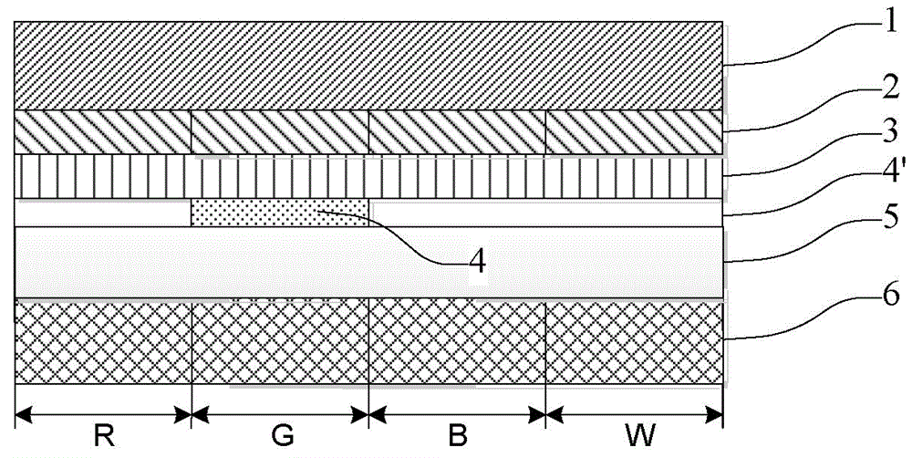
[0050] Such as figure 1 As shown, the OLED device with an optical resonant layer in this embodiment includes a substrate, a TFT array (not shown in the figure) is arranged on the substrate, a color filter film 6 is provided on the TFT array, and the color filter film 6 is divided into R , G, B, and W four colors to filter the white light emitted by the white OLED to form R sub-pixels, G sub-pixels, B sub-pixels and W sub-pixels. According to the needs, the R sub-pixel, G sub-pixel, B sub-pixel and W sub-pixel emit light of different intensities, and the light emitted by the R sub-pixel, G sub-pixel, B sub-pixel and W sub-pixel is mixed to obtain the required color. Display in color. After a plurality of OLED devices are arranged according to a certain rule (such as an array), they cooperate with other components such as a casing to form the display of the present invention.

[0051] figure 1In the illustrated embodiment, a planar layer 5 is provided on the color filter film...

no. 2 approach

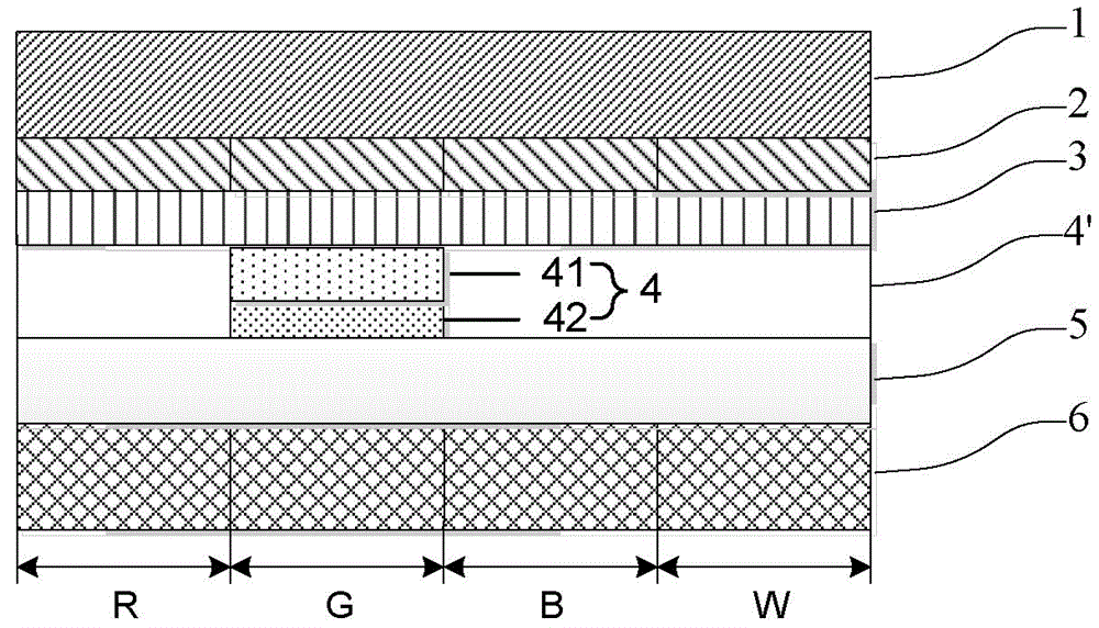
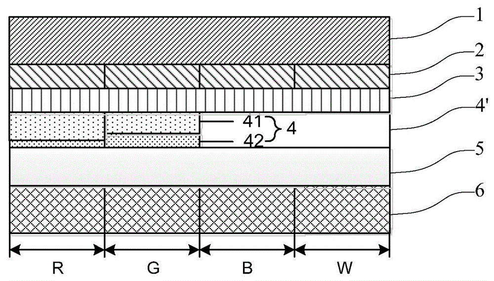
[0061] Such as figure 2 As shown, the difference between this embodiment and the first embodiment is that the optical resonant layer 4 has a double-layer dielectric structure. That is, the optical resonance layer 4 in the second embodiment includes the first dielectric layer 42 and the second dielectric layer 41 . The preparation method of the OLED device of the second embodiment is as follows:

[0062] 1. Clean the substrate and prepare a TFT array on the substrate;

[0063] 2. Prepare color filter film 6;

[0064] 3. Prepare a flat layer 5 on the color filter film 6;

[0065] 4. Prepare the first dielectric layer 42 in the area corresponding to the G sub-pixel on the flat layer 5, and prepare the second dielectric layer 41 on the first dielectric layer 42 to complete the preparation of the optical resonant layer 4 of the double dielectric layer structure; Area preparation filling layer 4';

[0066] 5. Prepare a transparent electrode 3 on the optical resonant layer 4 an...


PUM


Abstract

The invention discloses an OLED device with an optical resonance layer, a manufacturing method of the OLED device and a displayer. The OLED device comprises a white light OLED and a color filter film, the white light OLED and the color filter film are used for forming R sub-pixels, G sub-pixels, B sub-pixels and W sub-pixels, and the optical resonance layer is at least arranged between the white light OLED and the color filter film and corresponds the area of the G sub-pixels. According to the OLED device with the optical resonance layer, the optical resonance layer is arranged, so even if the color filter film low in color gamut is adopted, monochromatic light good in chroma and high in efficiency can be filtered out, and especially, the problem that display quality is low in the current white light OLED+CF technology is solved. In addition, the OLED device greatly reduces power consumption. No fine metal mask (FMM) is needed, so that process cost is reduced.

Description

technical field [0001] The invention relates to the field of OLED display technology, in particular to an OLED device with an optical resonant layer, a preparation method thereof, and a display including the OLED device. Background technique [0002] With the progress of science and technology, liquid crystal display (Liquid Crystal Display, LCD) has gradually replaced the traditional bulky cathode ray display (Cathode Ray Tube, CRT) because of its advantages of small size and light weight, and has been widely used Used in monitors, notebook computers, flat-panel TVs, digital cameras and other electronic products. [0003] The LCD requires a light emitting diode (Light Emitting Diode, LED) as a backlight source. Organic Light Emitting Diode (OLED) displays do not require a backlight module, are more suitable for thin displays, and have the advantage of no viewing angle restrictions, so they tend to replace traditional CRTs and LCDs. [0004] OLED displays include RGB displ...

Claims


Application Information

Patent Timeline
Patent Type & Authority Applications(China)
IPC IPC(8): H01L51/52H01L51/56H01L27/32
CPCH10K59/00H10K50/86H10K71/00H10K59/30H10K59/351H10K59/38H10K59/124H10K50/852H10K50/856H10K59/88H10K50/858
Inventor 李梦真刘嵩高松敖伟周斯然
Owner BEIJING VISIONOX TECH
Why Eureka
Try Eureka