A photoresist plate moving device

A technology of photolithography and forward and backward movement, applied in the direction of transportation and packaging, conveyor objects, etc., can solve problems such as insufficient stability, and achieve the effects of improving handling efficiency, accurate position, and reducing adsorption

Active Publication Date: 2017-01-04
NANTONG FUJITSU MICROELECTRONICS
View PDF10 Cites 0 Cited by
  • Summary
  • Abstract
  • Description
  • Claims
  • Application Information

AI Technical Summary

Problems solved by technology

[0003] In order to overcome the problems of cleanliness, accuracy, handling efficiency and insufficient stability in the process of transporting photoresist plates, the present invention provides a photoresist plate transporting device

Method used


Image

  • A photoresist plate moving device
  • A photoresist plate moving device
  • A photoresist plate moving device

Examples


Embodiment Construction

[0038] The present invention will be described in further detail below in conjunction with the accompanying drawings and embodiments. It should be understood that the specific embodiments described here are only used to explain the present invention, not to limit the present invention.

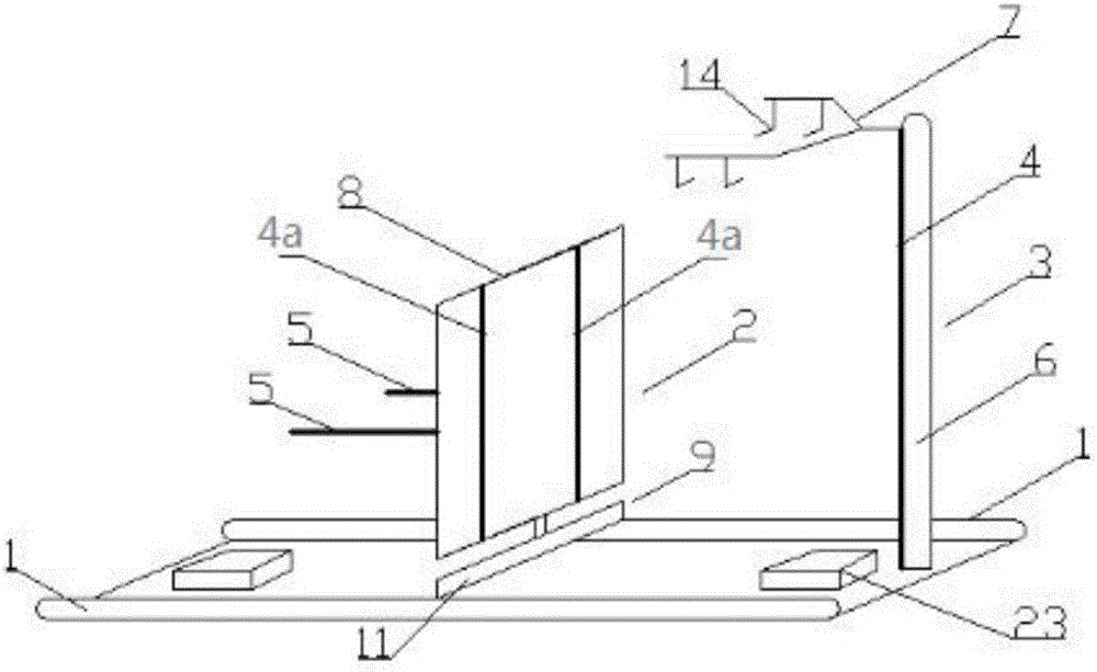
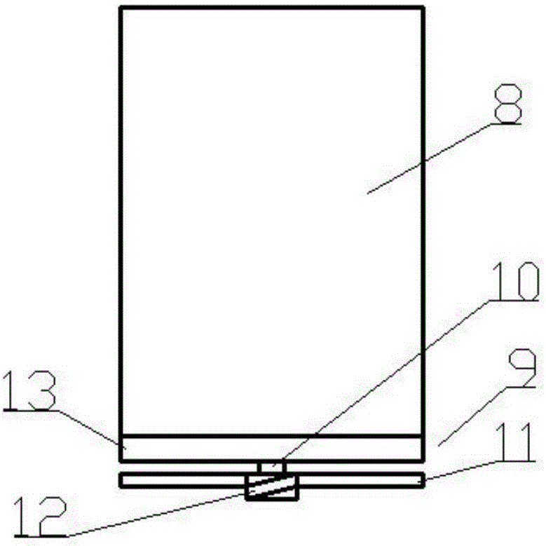
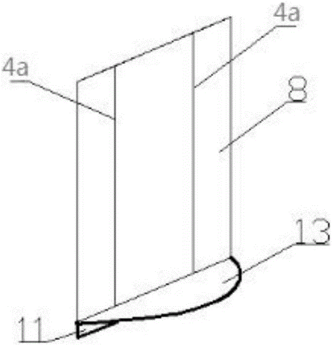
[0039] In another embodiment of the present invention, a photoresist plate moving device is provided, such as figure 1 , figure 2 , image 3 , Figure 4 As shown, it includes the slide rails 1 on both sides of the platform, the conveying part 2, the clamping part 3, the lower ends of the bottom 2 of the conveying part 2 are provided with buckles, the slide rail 1 is provided with a card slot, and the conveying part 2 can be placed on the slide rail 1 Moving up and down, the conveying part 2 is provided with a conveying guide rail 4a, and the conveying arm 5 can move up and down on the conveying guide rail 4a. The clamping part 3 includes a column 6 and a clamping arm 7 . The column 6 has ...


PUM


Abstract

The invention discloses a photo-etching plate carrying device. The photo-etching plate carrying device comprises sliding rails (1) on two sides of a platform, a carrying part (2) and a clamping part (3), wherein buckles are arranged at the lower ends of two heads of the bottom part of the carrying part (2); clamping slots are formed in the sliding rails (1); the carrying part (2) can move forwards and backwards on the sliding rails (1); the clamping part (3) comprises a vertical pillar (6) and a clamping arm (7); a guide rail (4) is arranged on the vertical pillar (6); the clamping arm (7) can move up and down on the guide rail (4); the carrying part (2) is provided with a guide rail (4) and a carrying arm (5); the carrying arm (5) can move up and down on the guide rail (4). By adopting the photo-etching plate carrying device, a semiconductor production line photo-etching plate simply and quickly converts and moves in a non-artificial contact manner between different storage boxes; the dust is reduced; the pollution and the damage caused by contact of fingers can be avoided; meanwhile, the photo-etching plate carrying device is more accurate and efficient.

Description

technical field [0001] The invention relates to the semiconductor industry, in particular to a transport device for transporting photoresist plates. Background technique [0002] In the semiconductor industry, photoresist plates are shipped from plate manufacturers using special storage boxes for transportation. After arriving at the fab, they must be transferred to special storage boxes that can be used by the lithography machine. Sometimes, the photoresist plates in the fab are transferred Manual contact is used to pick and place by hand, and this contact type has a great risk of falling on the one hand, and on the other hand, it will introduce more contact contamination. In the semiconductor manufacturing process, every link has high requirements on the cleanliness of the environment and equipment. Even a little bit of contamination will have an important impact on the quality of the product, so every detail is controlled very carefully. Important, among which the cleanl...

Claims


Application Information

Patent Timeline
Patent Type & Authority Patents(China)
IPC IPC(8): B65G47/74
Inventor 丁万春
Owner NANTONG FUJITSU MICROELECTRONICS
Why Eureka
Try Eureka