Process method for integrated circuit carrying plate plug hole
A technology of integrated circuits and process methods, applied in printed circuits, printed circuit manufacturing, electrical components, etc., can solve the problems of ink surface depression and high product defect rate, achieve high fullness, reduce product defect rate, and avoid duplication. printing effect
- Summary
- Abstract
- Description
- Claims
- Application Information
AI Technical Summary
Problems solved by technology
Method used
Image
Examples
Embodiment Construction
[0032] The following will clearly and completely describe the technical solutions in the embodiments of the present invention with reference to the accompanying drawings in the embodiments of the present invention. Obviously, the described embodiments are only some, not all, embodiments of the present invention. Based on the embodiments of the present invention, all other embodiments obtained by persons of ordinary skill in the art without making creative efforts belong to the protection scope of the present invention.
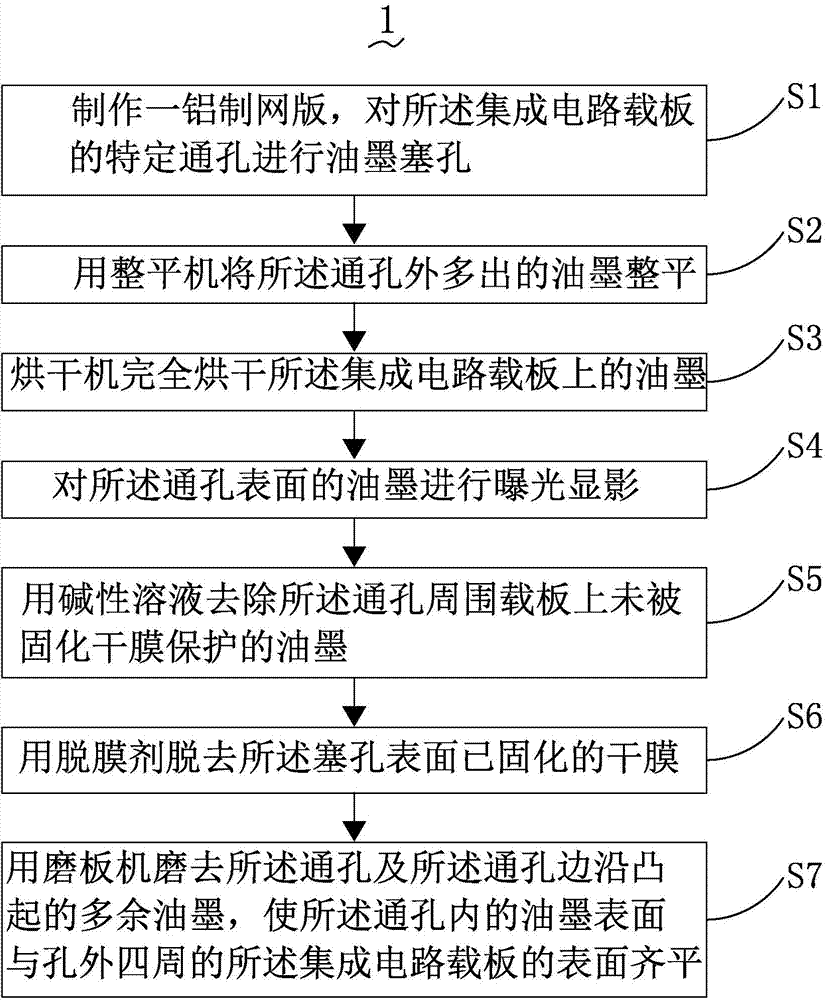
[0033] see figure 1 , is a flow chart of the steps of the process method for plugging holes of the IC substrate provided by the present invention. The method comprises the steps of:
[0034] Step S1, making an aluminum screen plate, and performing ink plugging on the specific through hole of the IC carrier board;
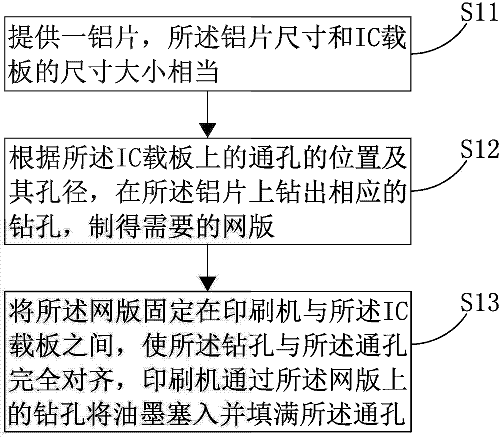
[0035] Specifically, see figure 2 , is the flow chart of screen making and ink plugging:
[0036] S11, provide an aluminum sheet, the size of ...
PUM
 Abstract
Description
Claims
Application Information


