Method for forming double pattern

A double-patterned and patterned technology, applied in electrical components, semiconductor/solid-state device manufacturing, circuits, etc., can solve the problems of double-pattern deformation, affecting the accuracy of etching patterns, etc., to avoid tilting or collapse and ensure accuracy. Effect

Inactive Publication Date: 2015-04-15
SEMICON MFG INT (SHANGHAI) CORP
View PDF7 Cites 9 Cited by
  • Summary
  • Abstract
  • Description
  • Claims
  • Application Information

AI Technical Summary

Problems solved by technology

[0011] The double pattern formed by the prior art is prone to deformation, which affects the accuracy of the etching pattern formed by subsequent etching of the etching material layer

Method used


Image

  • Method for forming double pattern
  • Method for forming double pattern
  • Method for forming double pattern

Examples


Embodiment Construction

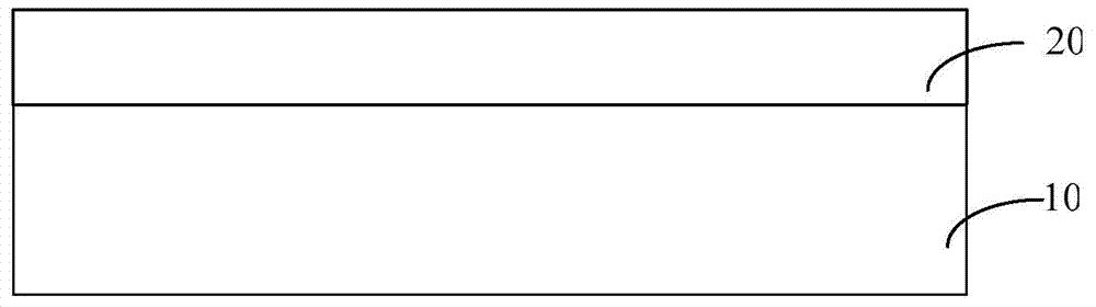
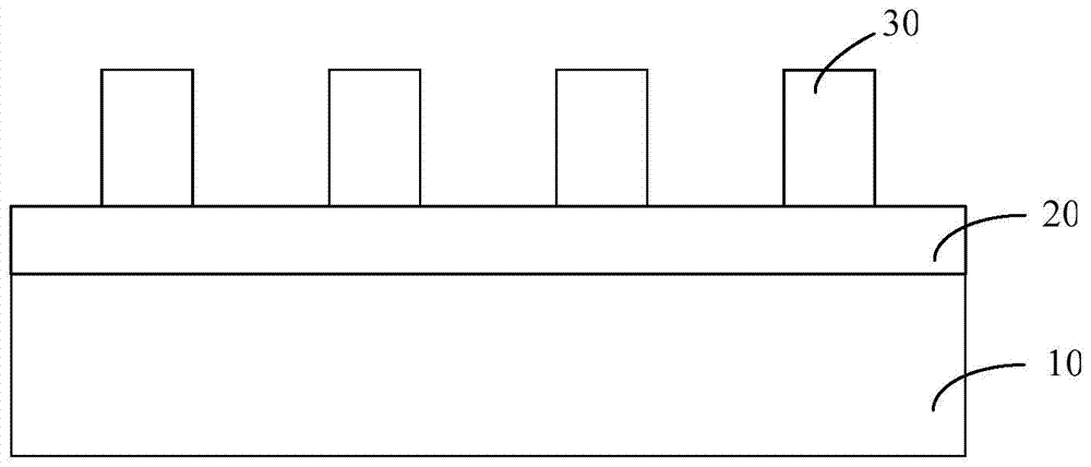
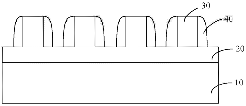
[0038] As mentioned in the background art, the double pattern structure formed in the prior art is prone to deformation, which affects the accuracy of the subsequently formed etching pattern.

[0039] Research has found that in the prior art, the ashing process is usually used to remove the sacrificial layer, and after the ashing process is performed to remove the sacrificial layer, the residual material of the sacrificial layer must be removed by solution cleaning to avoid the impact of residual particles on the subsequent process is affected. After cleaning, further drying treatment is required to remove the residual aqueous solution on the sidewall and the surface of the layer to be etched. Since the material of the sidewalls is mostly silicon oxide or silicon nitride, and the silicon oxide or silicon nitride is a hydrophilic material, during the drying process, as the aqueous solution between adjacent sidewalls gradually decreases , due to the hydrophilic effect between t...


PUM


Abstract

A method for forming a double pattern comprises the following steps: providing a layer to be etched; forming a sacrificial layer with openings on the surface of the layer to be etched, wherein the openings expose part of the surface of the layer to be etched; forming a spacer on the surface of each side wall of the sacrificial layer; removing the sacrificial layer; carrying out hydrophobic treatment on the spacers to enable the spacers to have a hydrophobic surface; and cleaning and drying the surface of the layer to be etched and the surfaces of the spacers. By adopting the method, the accuracy of a formed double pattern can be improved.

Description

technical field [0001] The invention relates to the technical field of semiconductors, in particular to a method for forming a double pattern. Background technique [0002] With the continuous shrinking of the minimum line width and spacing of integrated circuit design, when the feature size of the exposure line is close to the theoretical resolution limit of the exposure system, the imaging on the surface of the silicon wafer will be seriously distorted, which will lead to the deterioration of the quality of the lithography pattern. Seriously down. For example, etching the fin portion of the fin field effect transistor with smaller features will seriously affect the performance of the formed fin field effect transistor due to the degradation of the pattern quality. [0003] In order to reduce the impact of the optical proximity effect, the industry has proposed lithography resolution enhancement technology (RET), among which the much-concerned dual patterning technology (D...

Claims


Application Information

Patent Timeline
Patent Type & Authority Applications(China)
IPC IPC(8): H01L21/027
Inventor 三重野文健
Owner SEMICON MFG INT (SHANGHAI) CORP
Why Eureka
Try Eureka