Hardware acceleration method for predication of RNA second-stage structure with pseudoknot

A secondary structure, hardware acceleration technology, applied in special data processing applications, instruments, electrical digital data processing, etc., can solve problems such as high space-time complexity, no hardware acceleration of high-dimensional four-dimensional structure prediction algorithms, and poor prediction results.

Inactive Publication Date: 2015-04-22
NAVAL UNIV OF ENG PLA
3 Cites 10 Cited by

AI-Extracted Technical Summary

Problems solved by technology

At present, although there are many improved algorithms based on PKNOTS that can support false knot prediction, these algorithms have sacrificed accuracy and correctness for execution speed, and the prediction effect is not good; Weight matching algorithms, while having ideal computational complexity, only have good predictive results for specific types of false knots
In comparison, the prediction effect of the PKNOTS algorithm is significantly better than other algorithms, but the high space-time complexity limits the practicability of the PKNOTS algorithm. Currently, it can only predict short sequence structures containing dozens of bases
[0022] In 2010, based on the IBM Cell multi-core processor, Krishnan et al. conducted...

Method used

Comparing table 1 and table 2 can be found, because there is no data correlation in the first two items in table 1, so it is merged; And the operand source of two groups of addition operations partially overlaps, all depends on the Cell( of YHX matrix 1,1) so merge it. Observing the adjacent entries in the operand source column in Table 2, it can be found that both YHX(1,1) and WHX(1,1) are used by adjacent operations, so they are marked. If the same data source is used by adjacent operations, it means that it can be cached on-chip during storage scheduling, and the off-chip storage access overhead can be reduced through data reuse.
[0089] The calculation array is composed of seven PE modules, which respectively realize the calculation of seven free energy matrices. All PEs are equal in status and are connected to the data bus. Each computing module has independent input and output data caches (Data Buf and Cache), where Data Buf is used to cache data loaded from off-chip, Cache is used to store the calculation results of this module, all PE calculation logic and The output data caches are all connected through the data transfer network and reused through data sharing. The data cache of the entire computing array and the unique data cache of the PE are implemented by the multi-port BlockRAM storage block on the FPGA chip. In order to avoid access conflicts, each computing module saves a copy of the RNA sequence and free energy parameter table, which is implemented using distributed storage resources on the FPGA chip. In addition, a data transfer register set is designed betw...

Abstract

The invention discloses a method for accelerating the predication of an RNA second-stage structure with pseudoknot based on a four-dimensional dynamic planning method, and aims at accelerating the predication of the RNA second-stage structure with pseudoknot. According to the technical scheme, the method comprises the steps of building a heterogeneous computing system through a host and a reconfigurable algorithm accelerator; sending parameters of a formatted thermodynamic model and coded RNA sequences to the reconfigurable algorithm accelerator through the host; computing seven computing modules of the algorithm accelerator through the non-backtracking PKNOTS algorithm by the MPMD mode; when in computing, a four-dimensional matrix is decomposed by the rectangular dimension reduction method into N three-dimensional matrixes, then the fine granularity is achieved by the task dividing strategy of circularly dividing in each layer by areas and parallelly processing by rows in the area, and the computing is carried out synchronously; for n PE in each computing module, n data in different rows of the area are computed synchronously through the SPMD mode. With the adoption of the method, the predication of the RNA second-stage structure with pseudoknot is accelerated; the technology is novel, the performance is high, and the cost is low.

Application Domain

Special data processing applications

Technology Topic

Hardware accelerationAlgorithm acceleration +14

Image

  • Hardware acceleration method for predication of RNA second-stage structure with pseudoknot
  • Hardware acceleration method for predication of RNA second-stage structure with pseudoknot
  • Hardware acceleration method for predication of RNA second-stage structure with pseudoknot

Examples

  • Experimental program(1)

Example Embodiment

[0050] The present invention will be further described below in conjunction with embodiments:
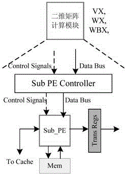
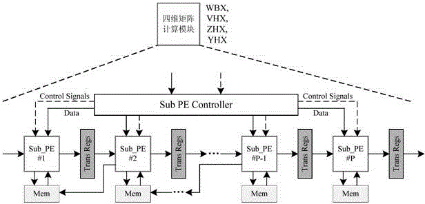
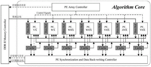
[0051] The present invention first constructs a heterogeneous computing system composed of a host computer and a reconfigurable algorithm accelerator, and then the host sends the formatted thermodynamic model parameters and the encoded RNA sequence to the reconfigurable algorithm accelerator, the seven computing modules of the algorithm accelerator The MPMD method is used to perform the PKNOTS algorithm calculation without backtracking; in the calculation, the matrix dimension reduction method is used to decompose the four-dimensional matrix into N three-dimensional matrices, and then the task division strategy of layer by layer by region rotation and column parallel processing in the region is used to achieve fine-grained tasks Parallel computing, n PEs in each computing module use SPMD to simultaneously compute n data in different columns in the area, where n is a natural number.
[0052] PKNOTS algorithm calculation is realized by three two-dimensional matrices and four four-dimensional matrix calculation modules, the three two-dimensional matrix calculation modules are PE_VX, PE_WX and PE_WBX; the four four-dimensional matrix calculation modules are PE_WHX, PE_VHX, PE_ZHX And PE_YHX. The parallel computing structure of seven modules (PE), such as Picture 10 Shown. Each PE is responsible for the calculation of a matrix. The module is named by PE_ followed by the name of the calculated matrix (for example, the module PE_VX means that the current PE is responsible for completing the calculation of the matrix VX).
[0053] Picture 10 The seven modules (PE) in the matrix form a PE array. The PE array simultaneously calculates the elements (i, j) with the same subscript in the seven matrices each time, which is an element for the two-dimensional matrix VX, WX and WBX, and For the four-dimensional matrix WHX, VHX, YHX, ZHX, it is Figure 7 One layer (that is, a triangular area) is called a "Cell".
[0054] The structures of the first three two-dimensional matrix calculation modules PE_VX, PE_WX and PE_WBX are exactly the same, and their internal structures are as Image 6 Shown. The two-dimensional matrix calculation modules PE_VX, PE_WX and PE_WBX all include a sub PE controller (Sub PE Controller), a sub PE calculation unit (Sub_PE), a local memory (Mem), and a data transfer register (Trans Regs). The connection relationship between the components such as Image 6 As shown, the arrow indicates the direction of data transfer. Among them, the Sub PE Controller is used to control the timing of calculation and data access; the core of the sub-PE calculation unit is a 32-bit adder, which is used to implement the addition operation of two input operands, and its calculation The result is written into the local memory (Mem) and the data transfer register at the same time. Among them, the local memory (Mem) is used to cache the calculation results of a whole column of elements in the two-dimensional matrix, and the data transfer register only stores the calculation results of the current element and is used by the next calculation module immediately.
[0055] The last four four-dimensional matrix calculation modules PE_WHX, PE_VHX, PE_ZHX and PE_YHX have exactly the same structure, and their internal structure is as Picture 9 Shown. Each calculation module contains a linear PE array. Since the function of the four-dimensional matrix calculation module is to realize the parallel calculation of the two-dimensional "Cell", and each Cell is a two-dimensional triangular matrix, it uses Picture 9 The shown multi-PE linear array structure adopts the strategy of "rotating and dividing by column" to realize the parallel calculation of multi-column elements. Picture 9 The structure of all the sub-processing units constituting the PE array is exactly the same, and its internal structure is the same as Picture 9 The sub-modules shown have the same structure. The Sub PE Controller (Sub PE Controller) implements task allocation, and loads the calculation tasks of one column of elements in the triangular matrix to the corresponding sub processing unit (Sub PE) each time, and controls the synchronization of the array. After the calculation is started, each sub-PE unit in the array calculates an element in the current column at a time, so that the entire array is viewed as a whole, and the correctness is achieved. Picture 8 (b) Synchronous calculation of a diagonal line in a certain area of ​​the subgraph. With the upward displacement of the unit currently calculated by each sub-PE, the diagonal line currently calculated by the entire PE array also moves upward, thus gradually realizing the parallel calculation of the two-dimensional "Cell".
[0056] The present invention adopts a data correlation analysis method called "spatio-temporal overlap", through program feature analysis to generate an operation execution sequence table, and extract data correlation from it; by performing multi-unit execution sequence items in time and The spatial domain merges and establishes the mapping relationship between the data source and the destination (discovering irrelevant operations through time domain overlap to achieve parallel computing; through spatial domain overlap to find the same data source to achieve data reuse), and construct a memory access scheduling matrix to guide Data scheduling optimization and parallel strategy formulation.
[0057] Figure 5 It is the main process of the data correlation analysis method of "spatio-temporal overlap", which shows the generation process from source code to data loading and transmission schematic diagram. The process includes four steps: operation type and data source statistics, data correlation and operand source analysis, multi-unit execution sequence table merging, and generation of memory access scheduling matrix.
[0058] 1. Calculation type and data source statistics
[0059] For the processing unit corresponding to each matrix, list the operation types and data sources according to the execution order of the code in the software; if a loop statement is encountered, the loop will be expanded, and the "Cell" in the four-dimensional matrix will be used as the basic data block. Statistics and analysis of the change law of variables and data-related areas, draw the movement trajectory of the current element and the elements that the calculation depends on, and extract the data correlation; according to the data correlation, the operations in the code are numbered in order, and the operation types are listed , Data source and related serial number, generate the operation execution sequence table in the source code as shown in Table 1. The operation type column in Table 1 can indicate an operation or a group of operations of the same type in the loop body. The YHX(1,1) in the source of the operand indicates that the current operation depends on the data in the YHX matrix Cell(1,1), Para(1,1) indicates that the current operation depends on the parameter table (1,1) area The data. The column of related serial number indicates that the calculation result of the current operation will be used by the subsequent operation corresponding to the serial number, that is, there is a write-first-read correlation between the serial numbers. If this column is empty, it means that the operation does not depend on the result of the previous operation.
[0060] Table 1 Operation execution sequence table
[0061]
[0062] 2. Data correlation and operand source analysis
[0063] Table 1 reflects the serial execution process of the code, and the data dependency between operations can be obtained by analyzing Table 1. Next, the operations are relabeled according to the execution order under the condition of true data correlation, the operations with data-related operations are assigned the sequence numbers, the operations without data-related operations are assigned the same numbers, and then the operations with the same numbers are merged. Since operations with the same number mean that they can be executed in parallel, that is, the actual execution time of the group of operations is the same, so this step is called time overlap. Next, analyze the data source of the time overlapping operation, and merge the same items in the operand source column. The same data source for different operations in the same row means that the actual memory access addresses are the same or similar, and the accessed data belong to the same cell, so it can be regarded as memory accesses with overlapping address spaces. After the above two processing steps, the execution sequence table after the spatio-temporal overlap processing as shown in Table 2 is obtained. Finally, mark the same items between two adjacent rows in the operand source column of the sequence table.
[0064] Table 2 Sequence of execution after spatio-temporal overlap processing
[0065]
[0066] Comparing Table 1 and Table 2, we can find that because the first two items in Table 1 do not have data correlation, they are merged; and the sources of operands of the two sets of addition operations are partially overlapped, and both depend on the Cell(1,1) of the YHX matrix. ) So merge them. Observing the adjacent entries in the operand source column of Table 2, we can find that YHX(1,1) and WHX(1,1) are both used by adjacent operations, so they are marked. If the same data source is used by adjacent operations, it means that it can be cached on-chip during storage scheduling, and the off-chip storage access overhead can be reduced through data reuse.
[0067] 3. Multi-unit execution sequence table merge
[0068] Follow steps 1 and 2 to establish an operation execution sequence table for each processing unit, and then merge multiple tables to generate a table multi-unit execution sequence table. Table 3 side-by-side lists the execution sequence table of the three calculation modules, each module includes the data source and the serial number that represents the data.
[0069] Table 3 Multi-unit execution sequence table
[0070]
[0071] Since different calculation modules calculate elements with the same coordinates in different matrices at the same time, and store the results in the FPGA chip, if there is a data dependency between these elements, data reuse can be realized through the on-chip data transfer network without involving off-chip Storage scheduling issues, so this step does not consider the data correlation between computing modules. Therefore, there is a sequential relationship between the vertical operations of the same computing module in Table 2, and the horizontal operations of the same serial number can be executed in parallel.
[0072] Next, under the premise of ensuring that the relative execution order of each module remains unchanged, perform the time overlap operation again, and adjust the execution order of the calculation modules up and down, so that operations in different calculation modules but the same data source are located in the same row of the table as much as possible .
[0073] Table 4 Multi-unit execution sequence table after time overlap
[0074]
[0075] Comparing Table 3 and Table 4, it can be found that since the first operation of calculation module 2 and the third operation of calculation module 1 use ZHX(1,1), the first row of calculation module 2 in Table 3 is moved To the third row of Table 4, the calculation module 2 is idle for the first two execution time periods. For the same reason, the second operation of calculation module 3 is moved to the fourth row of Table 4, which is aligned with the second operation of calculation module 2. Since the first operation of calculation module 3 and the first operation of calculation module 1 both use YHX(1,1), Para(1,2), the position of the first row of calculation module 3 remains unchanged.
[0076] 4. Generate memory access scheduling matrix
[0077] On the basis of Table 4, the data source is merged again. First, the data sources that all calculation modules need to use in each row are sorted according to the execution sequence number, and the same data sources are merged horizontally, and the memory access schedule is generated according to the loading order of the data sources. Matrix; Secondly, consider the execution of memory access operations that are adjacent in time. If the same data source is used, then merge vertically, realize data reuse through the data cache inside the FPGA, avoid repeated loading, and finally generate the final memory access scheduling matrix . Table 5 is a schematic diagram of the memory access scheduling matrix. The vertical direction of the table is the data source address arranged in the load order, and the horizontal direction is the destination of data transmission. "1" means that the data on the left will be used by the corresponding calculation module, and "0" means The data on the left will not be used by the corresponding module. "●" indicates that the corresponding data block has been loaded into the FPGA and is in a valid state, and no longer needs to be loaded from outside the chip.
[0078] Table 5 Memory access scheduling matrix
[0079] Data Sources
[0080] The following factors need to be considered when generating the memory access scheduling matrix: (1) Data correlation, if the different data sources that the current calculation depends on are stored in different storage modules, they will be loaded from different channels at the same time; (2) If different If the data source is stored in the same storage module, load it in the order of use, and start the pipeline as soon as possible; (3) If there is no correlation between the use of the data source, load a large block of data first; (4) If the IO channel is free And if there is a free buffer in the FPGA, the next data block will be prefetched immediately.
[0081] Experimental results show that using the finally generated memory access scheduling matrix to guide off-chip storage access scheduling, data allocation and reuse can reduce memory access requests by about 50%, thereby effectively reducing storage access overhead.
[0082] Due to the small storage requirements and simple calculation process of the two-dimensional matrix VX, WX and WBX, they are stored in the FPGA chip, and there is no need to consider their calculation and storage issues when designing. The four-dimensional matrix WHX, VHX, YHX, ZHX The calculation of is the core of the PKNOTS algorithm. according to Figure 4 As shown in the data dependency relationship between the matrices, the WHX matrix is ​​at the core of the data dependency graph, so this section takes the WHX matrix as an example to illustrate the filling process of the four-dimensional matrix.
[0083] The four-dimensional triangular matrix WHX(i,j,k,l) ​​can be decomposed into N three-dimensional triangular matrices WHX i (j,k,l)(1≤i≤N), each three-dimensional matrix WHX i (j,k,l) ​​consists of N two-dimensional triangular matrices with side length N, and each two-dimensional upper triangular matrix corresponds to image 3 One of the Cells.
[0084] Such as Figure 7 As shown, the calculation process uses Cell as the basic unit, starting from WHX 1 The first layer (Cell 1 ) Start: When the matrix WHX 1 (j,k,l) ​​layer 1 WHX 1 (1,k,l) ​​After the calculation, calculate the second layer WHX 1 (2,k,l) ​​until WHX 1 The last layer is calculated; then calculate the second three-dimensional matrix WHX 2 The first layer, the second layer,..., the Nth layer; then calculate WHX 3 … Until the last matrix WHX N The Nth layer is finished. The dotted line in the figure and the numerical value in the upper right corner of the two-dimensional triangular matrix represent the calculation order of Cell.
[0085] WHX for each three-dimensional matrix in the four-dimensional matrix i (j,k,l) ​​calculation, using Picture 8 In the area division calculation strategy shown, each layer (Cell) is divided into several areas by column, and then the calculation is performed on each area. Picture 8 (a) Each layer of the three-dimensional matrix in the sub-picture is divided into three areas. The number of the area represents the calculation order of the corresponding area, and the dotted line with arrows represents the calculation order of the elements in each area. For the calculation of each area, follow Picture 8 The task distribution strategy of column rotation as shown in the sub-figure (b) uses multiple processing units in a bottom-to-up order along the diagonal of the matrix to achieve parallel calculation of the current area in the current Cell.
[0086] Correct Picture 8 (b) For each area shown in the sub-picture, each PE is responsible for calculating a column in the current area, and the column number of the element calculated by the PE corresponds to the sequence number of the PE in the array. The shaded p column elements in the figure represent the current calculation area, and they are simultaneously allocated to p PEs for parallel calculation. Each PE starts from the bottom position of the respective column and is calculated in the order from bottom to top. When the calculation of the current area is started, all the elements of the PE calculation are located on the main diagonal of the triangular matrix (the element marked with an asterisk in the figure represents the initial calculation position): PE_1 calculation element (k,l), the second PE calculation element (k+1,l+1),..., the p-th PE calculation element (k+p-1,l+p-1). According to the data relevance of the algorithm, the elements on the diagonal line do not have data correlation, so p elements on different PEs can be calculated in parallel. Moreover, since the calculation amount of the elements on the same diagonal is equal, all PEs can advance synchronously. At any time, the elements currently calculated by the PE array are always on the same diagonal of the matrix. Since the number of elements in each column of the triangular matrix is ​​not equal, when the row coordinate k=1 of the element calculated by the PE, the PE calculation is suspended and enters the waiting state (if the calculation result needs to be written back to the off-chip memory, the PE will issue a write in the waiting state Reply to request). All PEs in the array will enter the synchronization waiting state in sequence according to their numbers, and send write-back requests.
[0087] For the other three four-dimensional matrices VHX, YHX and ZHX, the same calculation sequence as WHX is used. For the three two-dimensional matrices VX, WX, and WBX, the calculation is performed column by column from left to right, and each column is filled in the order from bottom to top. In order to achieve parallel computing, this paper designs seven computing modules (PE), each PE is responsible for the calculation of a matrix. The PE array simultaneously calculates the units (i, j) with the same subscript in the seven matrices each time, which is an element for the two-dimensional matrix VX, WX and WBX, but for the four-dimensional matrix WHX, VHX, YHX, ZHX Yes Figure 7 One layer in the middle, namely a "Cell".
[0088] Picture 10 It is a four-dimensional dynamic programming algorithm parallel computing structure based on heterogeneous multi-PE linear arrays, which is mainly composed of array control modules, multi-PE computing arrays, storage modules, and array synchronization and write-back control modules. Among them, the array control module is responsible for the initialization of the computing array, task allocation and switching of the control computing area.
[0089] The calculation array is composed of seven PE modules, which respectively realize the calculation of the seven free energy matrices. The status of all PEs is equal, and they are all connected to the data bus. Each computing module has an independent input and output data cache (Data Buf and Cache), among which Data Buf is used to cache data loaded from outside the chip, Cache is used to store the calculation results of this module, and the calculation logic of all PEs The output data cache is connected through the data transmission network, and reuse is realized through data sharing. The data cache of the entire computing array and the unique data cache of PE are implemented using FPGA on-chip multi-port BlockRAM storage blocks. In order to avoid access conflicts, each computing module saves a copy of the RNA sequence and free energy parameter table, which is implemented using distributed storage resources on the FPGA chip. In addition, a data transfer register group is also designed between PEs to realize fast transfer of PE calculation results. The array synchronization and write-back control module is connected to the output cache and arithmetic logic of each PE, and is used to control the synchronization of the PE array and sequentially write the calculation results stored in the Cache back to the off-chip memory.
[0090] Comparative test: We implemented the hardware PKNOTS algorithm accelerator on the test platform. The test platform consists of a general-purpose computer and an algorithm accelerator. The host is configured with an Intel Core2 quad-core Q94002.66GHz processor with 4.0GB main memory. The algorithm accelerator hardware mainly includes a Xilinx Virtex7 series FPGA chip (XC7VX485T), three DDR3-1600DRAM memory sticks with a capacity of 8GB, and the accelerator is connected to the host through the SFP+ optical fiber data channel (implemented by the GTX Transceiver integrated inside the XC7VX485T chip), valid data The transmission bandwidth can reach 10Gb/s. The algorithm accelerator supports dynamic reconfiguration, which can complete fast switching between CM models of different scales within 60ms. Compared with conventional configuration methods such as JTAG or parallel SlectMAP with configuration time of seconds, the configuration efficiency of FPGA is improved by 2 to 3 Magnitude. The RNA secondary structure prediction software version is PKNOTS-1.08, developed by Elena Rivas of Washington University School of Medicine, and runs on three different platforms: Intel Core2 quad-core Q9400, Intel Xeon(R) X5670 CPU and FPGA algorithm accelerator.
[0091] The experimental results (Table 6) show that only one PKNOTS algorithm acceleration engine can be implemented on the XC7VX485T FPGA platform. The main reason is that the "Cell" data blocks of the four-dimensional matrix cache occupy too much storage capacity, and the utilization rate of storage resources has reached 82 %, while the logic resource utilization rate is only 28%. Since the operation type is mainly multiplication and addition operation, there are no large-scale multiplexers and centralized storage access ports in the design, and the system clock frequency can reach 210MHz. It can be seen that insufficient storage resources are the main bottleneck for system implementation. If you use the largest-scale commercial FPGA device XC6VSX1140T, at least two PKNOTS algorithm acceleration engines can be used, the structure prediction of two RNA sequences can be realized at the same time, and longer sequences can be supported.
[0092] Table 6 Implementation results of the four-dimensional dynamic programming algorithm on the FPGA platform
[0093]
[0094] Parallel effect
[0095] Table 7 PKNOTS algorithm acceleration effect (time unit: second)
[0096]
[0097] The experiment selected 4 sets of RNA sequences between 30 and 176bps, tested the average execution time of the PKNOTS-1.08 program on the Inter Q9400 and Intel Xeon(R)X5670 CPU platforms, and compared them with the hardware accelerator. It can be seen from Table 7 that the execution of the sequence structure prediction containing 30 bases on the algorithm accelerator can obtain a 2 times acceleration ratio, and when the test sequence length is 176 bps, a 51.8 times acceleration effect can be obtained. Compared with Intel Xeon(R)X5670, it can also get more than 25 times acceleration effect. Limited by the logic and storage capacity of the XC7VX485T FPGA device, it is currently only possible to predict the structure with pseudo-knots for sequences less than 256bps in length. The comprehensive results using the Xilinx EDA tool show that two PKNOTS acceleration engines can be implemented on the XC7VX1140T chip, and the structure prediction of the two sequences can be achieved at the same time. Compared with the current mainstream CPU platform, the acceleration effect can be more than 60 times.

PUM

no PUM

Description & Claims & Application Information

We can also present the details of the Description, Claims and Application information to help users get a comprehensive understanding of the technical details of the patent, such as background art, summary of invention, brief description of drawings, description of embodiments, and other original content. On the other hand, users can also determine the specific scope of protection of the technology through the list of claims; as well as understand the changes in the life cycle of the technology with the presentation of the patent timeline. Login to view more.
Why Eureka
Try Eureka