Structure of groove type MOSFET and manufacturing method

A manufacturing method and trench technology, applied in semiconductor/solid-state device manufacturing, electrical components, circuits, etc., can solve problems such as termination failure and breakdown voltage reduction

Inactive Publication Date: 2015-04-22
SHANGHAI HUAHONG GRACE SEMICON MFG CORP
View PDF4 Cites 5 Cited by
  • Summary
  • Abstract
  • Description
  • Claims
  • Application Information

AI Technical Summary

Problems solved by technology

[0004] In the Termination area, CT (Contact, contact hole) etching will be etched to the bottom of the polysilicon along the gap, and the subsequent CT implantation will penetrate the polysilicon and implant it into the bottom of the trench, which will cause Termination to fail and BV (breakdown voltage) to decrease.

Method used


Image

  • Structure of groove type MOSFET and manufacturing method
  • Structure of groove type MOSFET and manufacturing method
  • Structure of groove type MOSFET and manufacturing method

Examples


Embodiment Construction

[0039] In order to have a more specific understanding of the technical content, characteristics and effects of the present invention, now in conjunction with the accompanying drawings, the details are as follows:

[0040] The manufacture method of trench type MOSFET of the present invention, its specific processing steps are as follows:

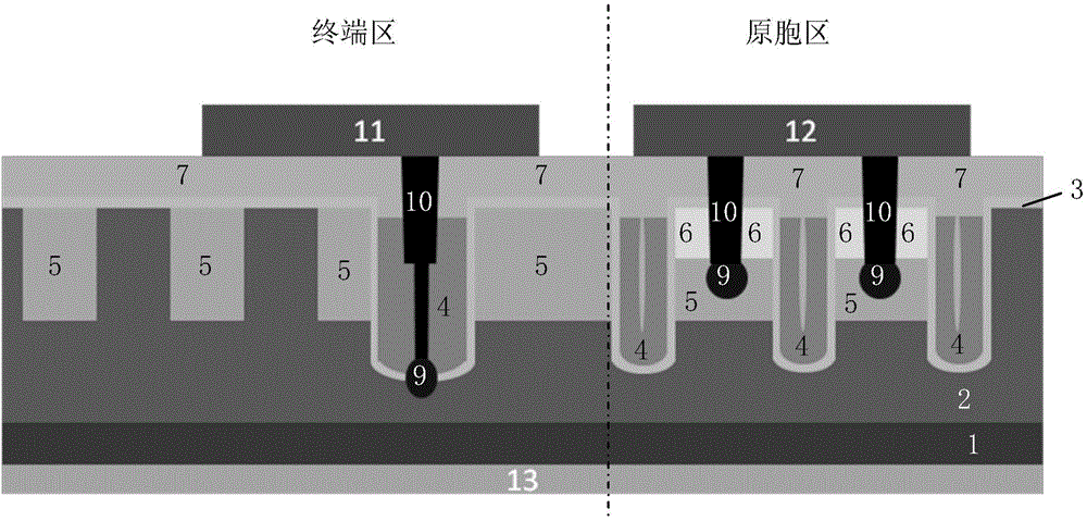
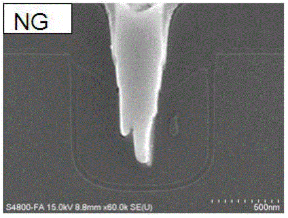
[0041] Step 1, etch a trench on the N-type epitaxy 2, such as Figure 5 shown. Among them, the inclination angle of the Gate Runner trench (gate channel trench) located in the terminal area is required to be between 87 and 89 degrees (the inclination angle can be adjusted by adjusting the pressure and gas flow rate of trench etching), such as Figure 10 As shown, other grooves located in the cell area are vertical grooves, and the depth of the grooves is determined according to product requirements.

[0042] Step 2, grow the gate oxide layer 3, deposit polysilicon 4, and then etch back to the gate oxide layer 3, such as Image 6 shown.

...


PUM

PropertyMeasurementUnit
Slopeaaaaaaaaaa

Abstract

The invention discloses a manufacturing method for a groove type MOSFET. The manufacturing method is characterized by comprising the steps that 1), a groove is etched, and side walls of the groove of a grid channel incline; 2), grid-oxide grows, and polycrystalline silicon is deposited and etched back; 3), injecting and annealing are carried out on a body region and a source region; 4), a dielectric medium between layers is deposited, and a contact hole is etched, injected and annealed; 5), a barrier layer of the contact hole is deposited, tungsten is deposited and etched back, top layer metal is deposited and etched to form a grid electrode and a source electrode, and back metal is deposited to form a drain electrode. The invention further discloses a structure of the MOSFET manufactured through the method. By optimizing the etching parameters of the groove, the vertical shape of the groove of the grid channel is adjusted to the inclining shape, the polycrystalline silicon filling the groove does not generate gaps after being etched back, the situation that CT etching is carried out downwards along the gaps in the polycrystalline silicon is avoided, and it is ensured that the edge of a device is not broken down.

Description

technical field [0001] The invention relates to the field of manufacturing semiconductor integrated circuits, in particular to a method for manufacturing a trench MOSFET (Metal Oxide Semiconductor Field Effect Transistor). Background technique [0002] Silicon-based power MOSFETs realize high-current operation by connecting a large number of MOS (metal-oxide-semiconductor) units in parallel. For MOSFET, the surface voltage between the parallel MOS units located in the middle of the device is roughly the same, but the voltage of the MOS unit located at the boundary (ie terminal) and the surface of the substrate is very different, which often causes the surface electric field to be too concentrated, causing the device edge breakdown. Therefore, in order to ensure the normal operation of silicon-based power MOSFETs, it is usually necessary to adopt Termination (terminal) technology at the device boundary to reduce the surface electric field intensity and increase the PN juncti...

Claims


Application Information

Patent Timeline
IPC IPC(8): H01L29/78H01L21/336
CPCH01L29/66666H01L29/7827
Inventor 丛茂杰许凯强徐俊杰
Owner SHANGHAI HUAHONG GRACE SEMICON MFG CORP
Why Eureka
Try Eureka