A three-dimensional stacked packaging structure and packaging method thereof

A technology of stacked packaging and packaging methods, applied in the direction of electrical components, electric solid devices, circuits, etc., can solve the problems of packaging trends that do not conform to miniaturization, shrink packaging volume, and difficult processes, etc., to achieve control of warping problems, The effect of simplifying the process and reducing the production cost

Active Publication Date: 2017-12-15
JIANGYIN CHANGDIAN ADVANCED PACKAGING CO LTD
View PDF4 Cites 0 Cited by
  • Summary
  • Abstract
  • Description
  • Claims
  • Application Information

AI Technical Summary

Problems solved by technology

In order to avoid interference between the chip on the first layer and the carrier board on the second layer, this method requires the use of large-sized solder balls, and larger solder balls require a larger space to prevent short circuits between solder balls, so this method The welding density is low and the process is difficult, which is not conducive to reducing the packaging volume and does not meet the trend of miniaturization packaging

Method used


Image

  • A three-dimensional stacked packaging structure and packaging method thereof
  • A three-dimensional stacked packaging structure and packaging method thereof
  • A three-dimensional stacked packaging structure and packaging method thereof

Examples


Embodiment 1

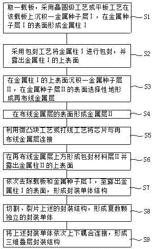
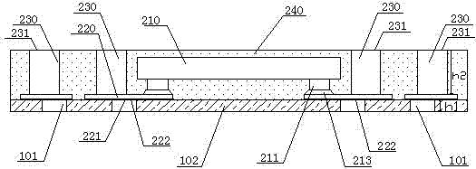
[0067] Example 1, see image 3

[0068] See image 3 , image 3 It is a schematic cross-sectional view of a package structure using micro bumps to form an electrical interconnection between a chip and a package body of the present invention.

[0069] by image 3 It can be seen that the structure of the package monomer of the present invention includes a chip package body and a lower package body. The lower package body is located below the chip package body and is closely connected with the chip package body through a packaging process.

[0070] The chip 210 of the chip package is located in the center of the entire chip package, and the wiring metal layer 220 is selectively distributed around the chip 210. There may be more than one chip 210, and their models may be the same or different, and they may be arranged as required. Using the chip flip-chip process, the chip 210 and the near-chip end of the rewiring metal layer 220 are flip-chip connected to the rewiring metal layer 220 t...

Embodiment 2

[0085] Example two, see Image 6

[0086] See Image 6 , Image 6 It is a schematic cross-sectional view of a package structure using wire bonding to form electrical interconnections between the chip and the package body of the present invention.

[0087] by Image 6 It can be seen that the structure of the package monomer of the present invention includes a chip package body and a lower package body, and the lower package body and the chip package body are tightly connected through a packaging process.

[0088] The chip 210 of the chip package is located in the center of the entire chip package, and the wiring metal layer 220 is selectively distributed around the chip 210. There may be more than one chip 210, and their models may be the same or different, and they may be arranged as required. Using a wire bonding process, the electrode of the chip 210 and the near-chip end of the rewiring metal layer 220 are connected by metal leads 280 to form an electrical interconnection. The m...


PUM


Abstract

The invention discloses a three-dimensional laminated packaging structure and a packaging method thereof, belonging to the technical field of semiconductor packaging. It includes a plurality of packaging monomers packaged up and down. The packaging monomer includes a chip package and a lower package. The chip package includes at least one chip and a rewiring metal layer. The lower surface of the rewiring metal layer is provided with the chip package. The lower input / output terminal is on the same side of the chip, and the far chip end of the rewiring metal layer is provided with metal pillar II, and the metal pillar II is fixedly connected with the rewiring metal layer to form the upper input / output end of the chip package; the lower package The metal pillar I is fixedly connected to the lower input / output end of the chip package, and the encapsulation material layer I encapsulates the metal pillar I, and exposes the lower surface of the metal pillar I, forming the input / output end of the lower package body; adjacent up and down The two package monomers are connected by solder balls / solder bumps. The three-dimensional stacked packaging structure formed by the invention does not need a carrier board to carry chips, has a simple structure, and conforms to the development trend of miniaturization.

Description

Technical field [0001] The invention relates to a three-dimensional stacked packaging structure and a packaging method thereof, and belongs to the technical field of semiconductor packaging. Background technique [0002] As the main method of packaging high-density integration, the package body stack in the three-dimensional stacked packaging structure has become the industry's first choice. [0003] In the existing package stacked package structure, as the unit of package stacked package, each independent package needs to use the film substrate as the package carrier to carry the packaged chip. The structure complex. Such as figure 1 Shown is a typical two-layer stack package design. The second layer package 13 is soldered to the first layer package 11 through the reflow process of solder balls 12. The above process can be repeated for more layers of stacked package design. In order to avoid interference between the chip on the first layer and the carrier board on the second lay...

Claims


Application Information

Patent Timeline
Patent Type & Authority Patents(China)
IPC IPC(8): H01L23/482H01L23/488H01L23/498H01L21/48H01L21/60
CPCH01L2224/16225H01L2224/48091
Inventor 龙欣江毕金栋徐虎高军明张黎陈栋郭洪岩郭亮章力梅万元陈锦辉赖志明
Owner JIANGYIN CHANGDIAN ADVANCED PACKAGING CO LTD
Why Eureka
Try Eureka