Deep-groove power MOS (metal oxide semiconductor) device with ultrahigh cellular density and manufacturing method of deep-groove power MOS device

A technology for MOS devices and manufacturing methods, which is applied in the manufacturing of semiconductor/solid-state devices, electrical components, semiconductor devices, etc., can solve problems such as difficulty in further reduction, and achieve lower characteristic on-resistance, lower channel resistance, and cell density. improved effect

Active Publication Date: 2015-04-29
WUXI NCE POWER
View PDF4 Cites 10 Cited by
  • Summary
  • Abstract
  • Description
  • Claims
  • Application Information

AI Technical Summary

Problems solved by technology

At present, the domestic mass production process can expose and maintain the minimum cell trench line width of about 0.25 μm after etching. After the final etching and fabrication of sacrificial oxide layer and insulating gate oxide layer, the trench line width is about 0.4 μm. The line width of the minimum cellular contact hole that can be exposed in dom

Method used


Image

  • Deep-groove power MOS (metal oxide semiconductor) device with ultrahigh cellular density and manufacturing method of deep-groove power MOS device
  • Deep-groove power MOS (metal oxide semiconductor) device with ultrahigh cellular density and manufacturing method of deep-groove power MOS device
  • Deep-groove power MOS (metal oxide semiconductor) device with ultrahigh cellular density and manufacturing method of deep-groove power MOS device

Examples


Embodiment Construction

[0053] The present invention will be further described below in conjunction with specific drawings and embodiments.

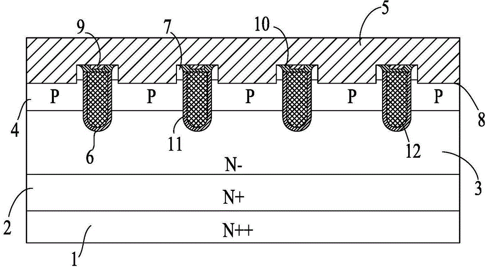
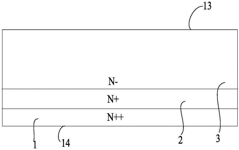
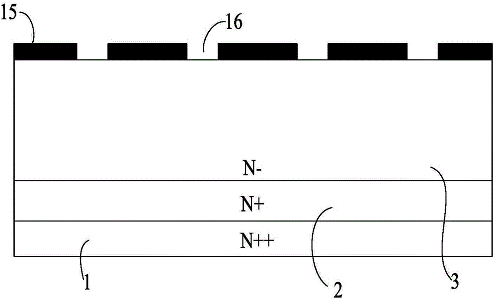
[0054] Such as figure 1 and Figure 15 As shown: In order to greatly reduce the channel resistance of MOS devices, thereby reducing the characteristic on-resistance of the entire device, taking N-type power MOS devices as an example, the present invention includes a The cell area and the terminal protection area on the top, the cell area is located in the central area of ​​the semiconductor substrate, and the terminal protection area surrounds the cell area; on the cross-section of the power MOS device, the semiconductor substrate includes the upper N type epitaxial layer and the lower N-type drain region 1, the N-type drain region 1 is adjacent to the N-type epitaxial layer;

[0055] In the cell area, the upper part of the N-type epitaxial layer is provided with a P-type well layer 4, and the cell area includes a number of cells arranged in parallel. The cel...


PUM


Abstract

The invention relates to a deep-groove power MOS (metal oxide semiconductor) device with ultrahigh cellular density and a manufacturing method of the deep-groove power MOS device. Cells in a cellular area adopt groove structures, gate oxidation layers are grown on the section of the power MOS device and the inner wall and the bottom of cellular grooves, and conductive polycrystalline silicon is deposited in the cellular grooves. Thermal oxidation layers are arranged in notches of the cellular grooves, insulation medium layers are deposited on the thermal oxidation layers, and the insulation medium layers and the thermal oxidation layer are distributed in the notches of the cellular grooves only. On the section of the power MOS device, source contact holes extend into a second conductive type trap layer downwards from a first conductive type source electrode and are filled with source metal, and the source metal contacts with the first conductive type source area and the second conductive type trap layer. The deep-groove power MOS device is compact in structure, groove resistance of the MOS device can be greatly reduced, and characteristic conduction resistance of the integral device is reduced.

Description

technical field [0001] The invention relates to a power MOS device and a manufacturing method thereof, in particular to a deep trench power MOS device with ultra-high cell density and a manufacturing method thereof, belonging to the technical field of power semiconductor devices. Background technique [0002] Trench power MOS devices have the characteristics of high integration, low on-resistance, fast switching speed, and low switching loss, and are widely used in various power management and switching conversions. With the development of industry, global warming has caused the climate environment to become more and more severe, and countries have begun to pay more and more attention to energy conservation, carbon reduction and sustainable development. Therefore, the requirements for power consumption and conversion efficiency of power MOS devices are getting higher and higher. When the application frequency is not high, the power consumption is mainly determined by the con...

Claims


Application Information

Patent Timeline
IPC IPC(8): H01L29/78H01L21/336
CPCH01L29/0847H01L29/66537H01L29/66666H01L29/7827
Inventor 朱袁正冷德武
Owner WUXI NCE POWER
Why Eureka
Try Eureka