Sonos device manufacturing process method
A manufacturing process and device technology, applied in the field of SONOS device manufacturing process, can solve problems such as being susceptible to interference, selection tubes and storage tubes do not share source and drain regions, etc., to reduce area, realize self-aligned etching, and reduce selection. tube effect
- Summary
- Abstract
- Description
- Claims
- Application Information
AI Technical Summary
Problems solved by technology
Method used
Image
Examples
Embodiment Construction
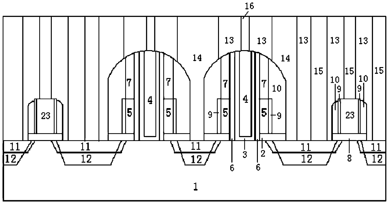
[0024] Described self-aligned SONOS device manufacture process method is in the following embodiment, implementation process is as follows:
[0025] Step 1, see Figure 4 A first oxide layer 17 is formed on the upper end of the P-type substrate 1, and the oxide layer 17 is used to finally form the gate oxide layer 8 of the transistor in the logic region and the gate oxide layer 2 of the selection transistor. A first polysilicon layer 18 and a first silicon nitride layer 22 are sequentially deposited on the first oxide layer 17, and the first polysilicon layer 18 is used to form the select transistor polysilicon gate 5 and the logic region transistor polysilicon Grid 23. The first silicon nitride layer 22 is used as a reserved layer of the CMP (chemical mechanical polishing) stop layer, and its deposited thickness is
[0026] Step 2, see Figure 5 , the photolithography is opened, the first silicon nitride layer 22 is etched, and the first polysilicon layer 18 is implanted...
PUM
 Abstract
Description
Claims
Application Information


