
Manufacturing process of SBR (sequencing batch reactor) device capable of realizing charge coupling through three-time masking

A manufacturing process and charge-coupled technology, which is used in semiconductor/solid-state device manufacturing, electrical components, semiconductor devices, etc., can solve the problems of high cost and rising device manufacturing cost, save costs, and save the step of annealing to form a source region. , to achieve the effect of self-aligned etching

Pending Publication Date: 2022-08-05
捷捷微电(上海)科技有限公司 +1
View PDF9 Cites 1 Cited by
  • Summary
  • Abstract
  • Description
  • Claims
  • Application Information

AI Technical Summary

Problems solved by technology

[0014] As we all know, the cost of setting up a mask is extremely high, and every time a mask is set up, the production cost of the entire device will greatly increase

Method used


Image

  • Manufacturing process of SBR (sequencing batch reactor) device capable of realizing charge coupling through three-time masking
  • Manufacturing process of SBR (sequencing batch reactor) device capable of realizing charge coupling through three-time masking
  • Manufacturing process of SBR (sequencing batch reactor) device capable of realizing charge coupling through three-time masking

Examples


Embodiment Construction

[0046] The technical solutions in the embodiments of the present invention will be clearly and completely described below with reference to the accompanying drawings in the embodiments of the present invention. Obviously, the described embodiments are only a part of the embodiments of the present invention, but not all of the embodiments. Based on the embodiments of the present invention, all other embodiments obtained by those of ordinary skill in the art without creative efforts shall fall within the protection scope of the present invention.

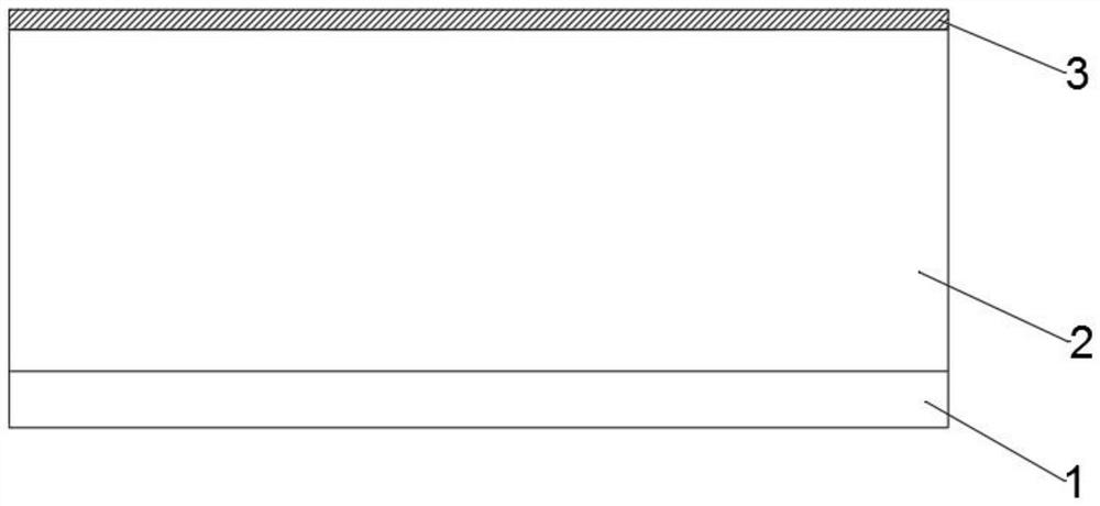
[0047] 2A to 2P A manufacturing process of a charge-coupled SBR device realized by three masks in this embodiment is shown, including the following steps:

[0048] Step 1: As Figure 2A As shown, a substrate 1 is provided, an epitaxial layer 2 is formed on the substrate 1, and a thin oxide layer 3 is formed on the surface of the epitaxial layer 2. In this embodiment, the thickness of the thin oxide layer 3 is 500A.

[0049] Step 2:...


PUM


Abstract

The invention discloses a manufacturing process of an SBR (sequencing batch reactor) device for realizing charge coupling through three-time masking. The manufacturing process comprises the following steps: forming a thin oxide layer; forming a body region; forming a thick oxide layer as a first mask; performing photoetching to form a groove; forming a field oxide layer; forming a first polycrystalline silicon; setting a second mask, and etching the first polycrystalline silicon to enable the top of the first polycrystalline silicon to be lower than the surface of the epitaxial layer; injecting source region ions by taking the thick oxide layer between the active region trenches as a mask; depositing to form a first oxide layer; and the first oxide layer is etched downwards in an isotropic manner, so that the epitaxial layer on the surface of the active region is exposed, an active region contact hole is formed in the active region trench, and the active region contact hole extends into the second polycrystalline silicon. According to the manufacturing process, the whole manufacturing process can be completed only through three times of mask, the mask needs to be arranged when the groove is formed, the first polycrystalline silicon is formed and the metal electrode is formed, the mask used when the source region is formed and the body contact region is formed is omitted, and cost is saved.

Description

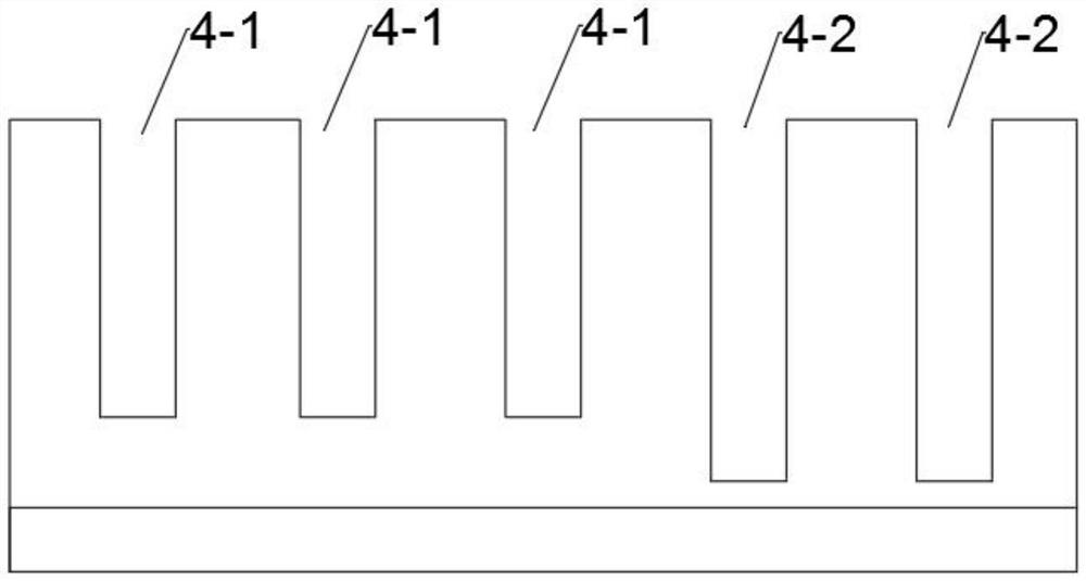
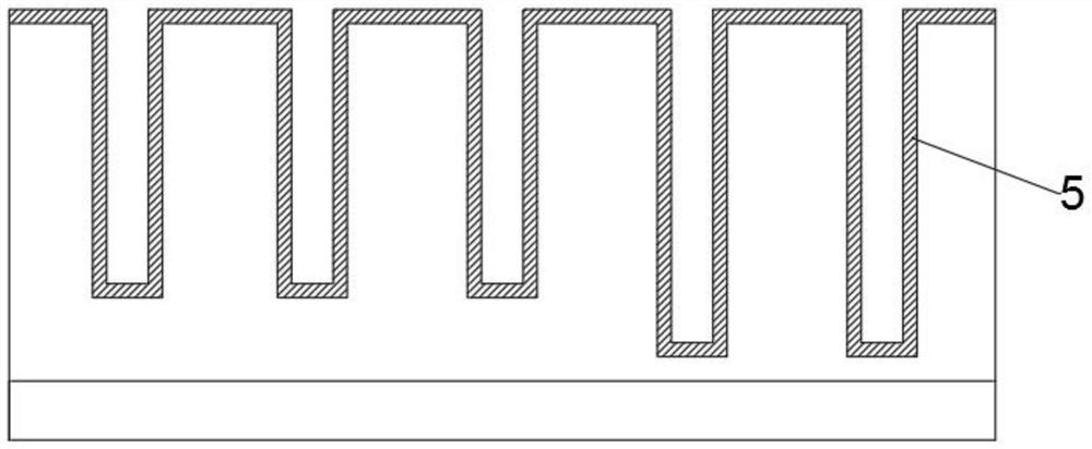
technical field [0001] The invention relates to the technical field of semiconductors, in particular to a manufacturing process of an SBR device in which charge coupling is realized by three masks. Background technique [0002] The fabrication process of traditional charge-coupled SBR devices is as follows: 1A to 1I shown, including the following steps: [0003] A substrate 1 is provided, an epitaxial layer 2 is formed on the substrate 1, and a thin oxide layer 3 is formed on the surface of the epitaxial layer 2, such as Figure 1A shown; [0004] A first mask is set, a trench is formed by photolithography, and the first mask is removed. The trench includes an active region trench 4-1 and a terminal region trench 4-2, such as Figure 1B shown; [0005] A field oxide layer 5 is formed in the trench, such as Figure 1C shown; [0006] Fill polysilicon and etch back to form a first polysilicon 6 in the trench, such as Figure 1D shown; [0007] A second mask 7 is set, t...

Claims


Application Information

Patent Timeline
Patent Type & Authority Applications(China)
IPC IPC(8): H01L21/336H01L29/423
CPCH01L29/66477H01L29/4236
Inventor 张楠黄健孙闫涛顾昀浦宋跃桦刘静吴平丽
Owner 捷捷微电(上海)科技有限公司
Learn More