This helps you quickly interpret patents by identifying the three key elements:
Problems solved by technology
Method used
Benefits of technology
Problems solved by technology
The main disadvantage of the existing technology is that it is difficult to form crystals with uniform size and controllable shape, so that the spectra obtained by the laser at different scanning times are not reproducible, and there is no quantitative relationship between signal intensity and sample volume
Moreover, due to the difference in crystal size and morphology, the initial velocity and direction of the ions obtained after the laser bombards the sample molecules are different, which affects the resolution and mass accuracy of the image.
In addition, these small organic molecule matrices often generate a series of background peaks in the low-mass region, suppressing low-mass molecular signals, and severely contaminating the ion source
Method used
Image
Click on the blue label to locate the original text in one second.
Reading with bidirectional positioning of images and text.
Examples
Embodiment 1
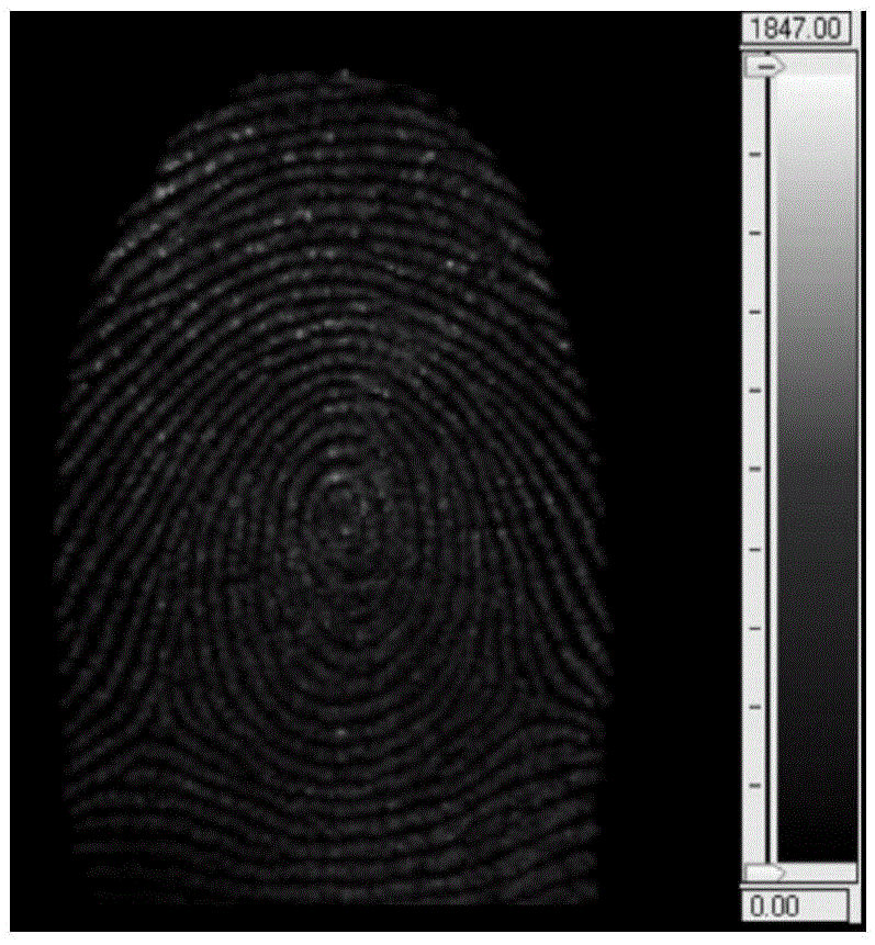
[0027] Preparation of high-resolution mass spectrometry imaging system image acquisition semiconductor thin film, which is used for imaging analysis of invisible fingerprints, the operation steps are as follows:
[0028] 1) Take a certain amount of (Bi) with an analytical balance 2 o 3 ) 0.07 (CoO) 0.03 (ZnO) 0.9 Semiconductor nanoparticles, such as 10mg, the type and amount of material can be determined according to different samples;
[0029] 2) burning the semiconductor nanoparticles obtained in step 1) in a muffle furnace at 350° C. for 1 hour to eliminate the pollution of the adsorbed organic molecules;
[0030] 3) The semiconductor nanoparticles obtained in step 2) are further ground with an agate mortar to make them uniformly dispersed;
[0031] 4) put the semiconductor nano-powder obtained in step 3) into the grinding tool of the tablet press, then put it into the tablet press, apply a pressure of 4800kg, and keep it under this pressure for 1 minute;
[0032] 5) ...
Embodiment 2
[0036] Preparation of high-resolution mass spectrometry imaging system image acquisition semiconductor film, which is used for mass spectrometry imaging of plant hormone jasmonic acid, the operation steps are as follows:
[0037] 1) Weigh a certain amount of (Bi2O3) with an analytical balance 0.07 (CoO) 0.03 (ZnO) 0.9 Semiconductor nanoparticles, such as 10mg, the type and amount of material can be determined according to different samples;
[0038] 2) burning the semiconductor nanoparticles obtained in step 1) in a muffle furnace at 350° C. for 1 hour to eliminate the pollution of the adsorbed organic molecules;
[0039] 3) The semiconductor nanoparticles obtained in step 2) are further ground with an agate mortar to make them uniformly dispersed;
[0040] 4) Put the semiconductor nano-powder obtained in step 3) into the grinding tool of the tablet press, then put it into the tablet press, apply a pressure of 2000kg, and keep it under this pressure for 1 minute to obtain a...
Embodiment 3
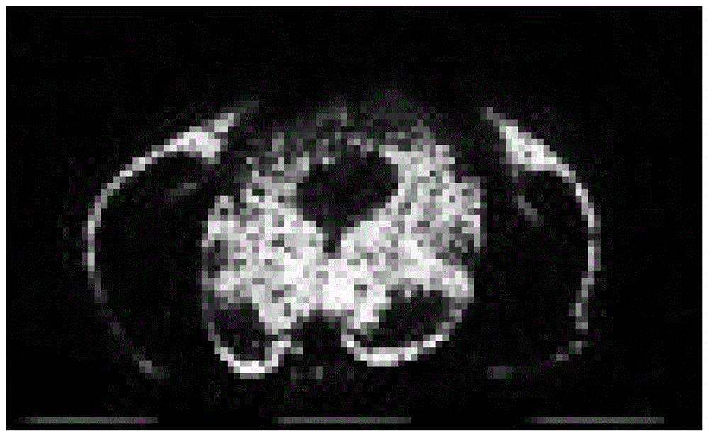
[0045] Preparation of semiconductor film for image acquisition of high-resolution mass spectrometry imaging system, which is used for mass spectrometry imaging of brain tissue cephalin, the operation steps are as follows:
[0046] 1) Weigh a certain amount of (Bi2O3) with an analytical balance 0.07 (CoO) 0.03( ZnO) 0.9 Semiconductor nanoparticles, such as 10mg, the type and amount of material can be determined according to different samples;
[0047] 2) burning the semiconductor nanoparticles obtained in step 1) in a muffle furnace at 350° C. for 1 hour to eliminate the pollution of the adsorbed organic molecules;
[0048] 3) The semiconductor nanoparticles obtained in step 2) are further ground with an agate mortar to make them uniformly dispersed;
[0049] 4) Put two-thirds of the semiconductor nano-powder obtained in step 3) into the grinding tool of the tablet press, then put it into the tablet press, apply a pressure of 4800kg, and keep it under this pressure for 1 minut...
PUM
Abstract
The invention belongs to the field of mass-spectral imaging, and in particular relates to an image acquisition semiconductor film for a high-resolution mass-spectral imaging system, and a preparation method and application of the image acquisition semiconductor film. The preparation method of the image acquisition semiconductor film for the high-resolution mass-spectral imaging system comprises the following steps: weighing semiconductor nano-particles, putting the semiconductor nano-particles into a muffle furnace for calcining firstly, further grinding by using an agate mortar, and uniformly dispersing the semiconductor nano-particles so as to obtain semiconductor nano-powder; and finally, pressing the semiconductor nano-powder in a tablet press so as to obtain the semiconductor film. By utilizing the laser-induced tunnel electron capture principle of a semiconductor nano-material, a sample is molecularized and ionized without background interference; the limitation of a conventional MALDI substrate is overcome; the semiconductor film is simple and easy to obtain, steady in mass-spectral signal, uniform and smooth in surface and free of the background interference, and can be used for fingerprint analysis and animal and plant tissue slice analysis; the semiconductor film is particularly applied to accurate mass-spectral imaging of small molecular substances; and quality control and industrialization are carried out conveniently.
Description
technical field [0001] The invention belongs to the field of mass spectrometry imaging, and in particular relates to a high-resolution mass spectrometry imaging system image acquisition semiconductor thin film, a preparation method and an application. Background technique [0002] Mass-assisted laser desorption dissociation mass spectrometry is an analytical technique commonly used in mass spectrometry imaging at present. This technology covers the surface of tissue slices with an organic small molecule matrix that can absorb laser energy, and transfers the energy to the sample molecules to vaporize and ionize them. detected by a mass analyzer. In this technique, the mixing mode of organic small molecule matrix and sample molecules is the key, because it directly affects the accuracy, resolution, reproducibility of experimental results and the ability of quantitative analysis of the analysis results. [0003] In the existing technology, an organic solvent is often used to d...
Claims
Application Information
Patent Timeline
Application Date:The date an application was filed.
Publication Date:The date a patent or application was officially published.
First Publication Date:The earliest publication date of a patent with the same application number.
Issue Date:Publication date of the patent grant document.
PCT Entry Date:The Entry date of PCT National Phase.
Estimated Expiry Date:The statutory expiry date of a patent right according to the Patent Law, and it is the longest term of protection that the patent right can achieve without the termination of the patent right due to other reasons(Term extension factor has been taken into account ).
Invalid Date:Actual expiry date is based on effective date or publication date of legal transaction data of invalid patent.

