P type transverse double-dispersion MOS pipe capable of reducing conduction resistance

A technology of lateral double diffusion and on-resistance, applied in circuits, electrical components, semiconductor devices, etc., can solve the problem of being difficult to make small, and achieve the effect of reducing the area of ​​the tube body

Inactive Publication Date: 2015-05-13
WUXI YOUDA ELECTRONICS
View PDF4 Cites 7 Cited by
  • Summary
  • Abstract
  • Description
  • Claims
  • Application Information

AI Technical Summary

Problems solved by technology

[0003] For P-type LDMOS devices, because they conduct electricity through holes, their on-resistance is even more difficult to

Method used


Image

  • P type transverse double-dispersion MOS pipe capable of reducing conduction resistance
  • P type transverse double-dispersion MOS pipe capable of reducing conduction resistance

Examples


Embodiment Construction

[0029] The technical solution of the invention will be described in detail below in conjunction with the accompanying drawings.

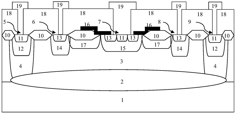
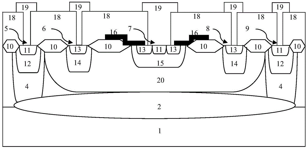
[0030] The P-type lateral double-diffused MOS transistor with reduced on-resistance involved in the present invention is as follows: figure 1 As shown, on a P-type substrate 1, a P-type epitaxial layer 3 is grown, and PLDMOS is formed in the epitaxial layer. Between the P-type substrate 1 and the P-type epitaxial layer 3 is an N-type buried layer 2 . At both ends of the N-type buried layer 2 are deep N wells 4 . The deep N well 4 diffuses 4~6um downward from the P-type epitaxial surface, communicates with the N-type buried layer, and isolates the inner P-type epitaxial layer from the outer P-type epitaxial layer to form an isolation structure. On the surface of the P-type epitaxial layer 3, a first active region 5, a second active region 6, a third active region 7, a fourth active region 8, and a fifth active region 9 are arranged in sequence. A ...


PUM

PropertyMeasurementUnit
Thicknessaaaaaaaaaa
Thicknessaaaaaaaaaa

Abstract

The invention discloses a P type transverse double-dispersion MOS pipe capable of reducing conduction resistance, and belongs to the technical field of semiconductor devices. The P type transverse double-dispersion MOS pipe capable of reducing conduction resistance comprises a P type substrate, an N embedded layer, a P type epitaxial layer, a first active area, a second active area, a third active area, a fourth active area, a fifth active area, field areas arranged between the active areas, a deep N trap, a shallow P trap, an N+ injection diffusion area, a shallow N trap, P+ injection diffusion area, and a P type injection layer which is between the shallow P trap and a back gate N trap area. With the adoption of the P type transverse double-dispersion MOS pipe, the conduction resistance is reduced while pressure resistance is ensured, and moreover, the area of a device is reduced.

Description

technical field [0001] The invention discloses a P-type lateral double-diffused MOS transistor with reduced on-resistance, belonging to the technical field of semiconductor devices. Background technique [0002] With the gradual development of lateral double-diffused MOS transistors (LDMOS), its performance such as high withstand voltage, good thermal stability, stable frequency, and higher gain has become increasingly prominent. LDMOS has become a key technology for high-voltage integrated circuits and power integrated circuits, and has been widely used It is used in aviation, spaceflight, control system, communication system, weapon system, etc. Therefore, LDMOS-based research has always been the focus and hot spot of research institutes, laboratories, electronic device manufacturers and colleges and universities all over the world. From a structural point of view, the electrodes of LDMOS devices are all located on the chip surface, which is easy to integrate with low-vol...

Claims


Application Information

Patent Timeline
IPC IPC(8): H01L29/78H01L21/336H01L29/41
Inventor 朱伟民邓晓军
Owner WUXI YOUDA ELECTRONICS
Why Eureka
Try Eureka