

Nanoimprinting method and device of array micro structure
A nano-imprinting and micro-structure technology, applied in the fields of nanotechnology, optics, opto-mechanical equipment, etc., can solve the problems of low processing efficiency, and achieve the effect of fast heating speed, precise control of heating area, and accurate construction
- Summary
- Abstract
- Description
- Claims
- Application Information
AI Technical Summary
Problems solved by technology
Method used
Image

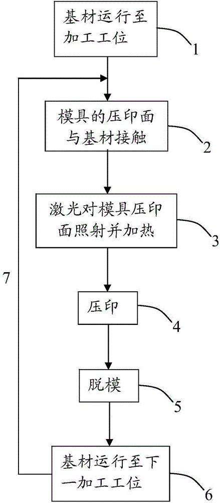
Examples
Embodiment 1
[0052] PMMA is used as the processing substrate, and the metal nickel material grating with a line width of 500nm is used as the needle tip indenter, and the microstructure grating array template is processed by the needle nanoimprinting method.
[0053] Specifically, the processing substrate is fixed on the workbench, and the imprinting surface of the microstructure mold having the above-mentioned needlepoint indenter is controlled to be in contact with the area to be processed; the heating laser is turned on, and the laser beam is focused and irradiated on the surface of the embossing surface , the focal spot size is 200um, the surface temperature rises through energy radiation, and the surface processing temperature is about 200°C.
[0054] When the surface temperature of the embossed surface reaches the processing temperature of the substrate, the embossing pressure is applied to the imprinted surface of the microstructure mold, and the pressure is maintained to promote the...
Embodiment 2
[0058] The PC is used as the processing base material, the silicon material device with the square boss structure is used as the pinpoint indenter, and the template of the nano pit of the Fabry-Perot optical resonant cavity is processed by the pin nanoimprinting method.
[0059] Specifically, the processing substrate is fixed on the workbench, and the imprinting surface of the microstructure mold having the above-mentioned needlepoint indenter is controlled to be in contact with the area to be processed; the heating laser is turned on, and the laser beam is focused and irradiated on the surface of the embossing surface , the focal spot size is 500um, the surface temperature rises through energy radiation, and the surface processing temperature is about 250°C.
[0060] When the surface temperature of the embossed surface reaches the processing temperature of the substrate, the embossing pressure is applied to the embossed surface of the microstructure mold, and the pressure is m...
Embodiment 3
[0064] The PMMA-MA copolymer is used as the processing substrate, and the metal nickel material grating with a line width of 600nm is used as the needle tip indenter, and the needle nanoimprinting method is used to process the holographic pattern template with a specific pattern.
[0065] Specifically, the processing substrate is fixed on the workbench, and the imprinting surface of the microstructure mold having the above-mentioned needlepoint indenter is controlled to be in contact with the area to be processed; the heating laser is turned on, and the laser beam is focused and irradiated on the surface of the embossing surface , the focal spot size is 100um, the surface temperature rises through energy radiation, and the surface processing temperature is about 180°C.
[0066] When the surface temperature of the embossed surface reaches the processing temperature of the substrate, the embossed surface of the microstructure mold is controlled to apply embossing pressure, and th...
PUM
| Property | Measurement | Unit |
|---|---|---|
| depth | aaaaa | aaaaa |
Abstract
Description
Claims
Application Information