

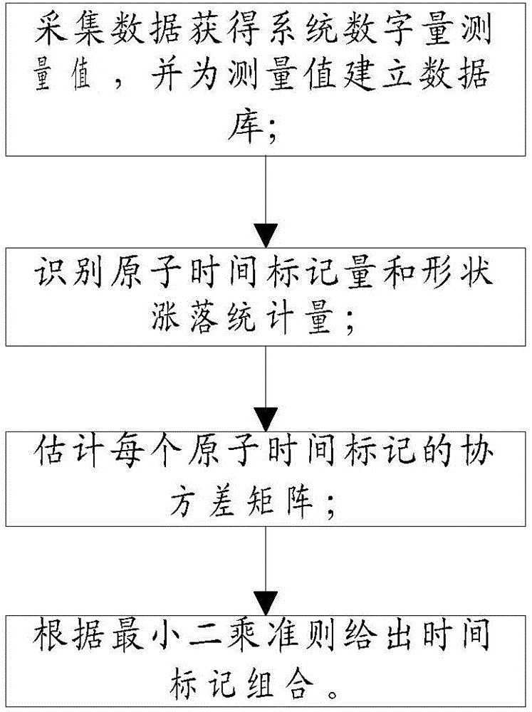
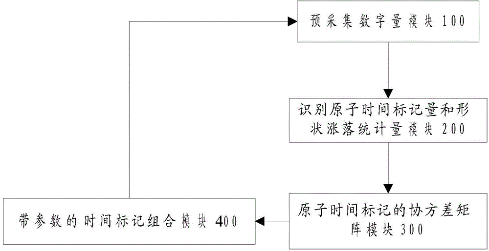
Time stamp combining method and system
A technology of time marking and atomic time marking, which is applied in the fields of digital signal processing, photoelectric signal processing and nuclear detection, can solve the problems of ultra-high data throughput and processing, high cost, etc., achieve good adaptability, good system, and improve system time resolution rate effect
- Summary
- Abstract
- Description
- Claims
- Application Information
AI Technical Summary
Problems solved by technology
Method used
Image

Examples
example 1
[0077] The parameters of data processing in this embodiment are listed here:
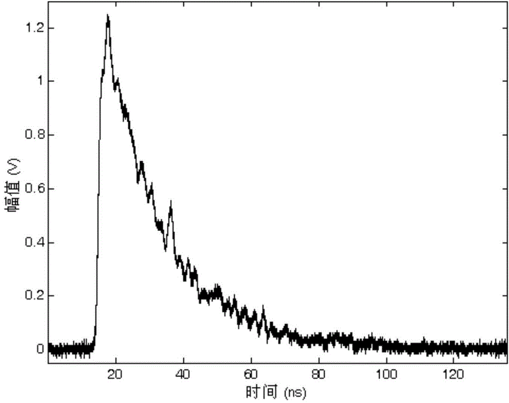
[0078] The actual system used in step (1) used LaBr crystal and Hamamatsu R9800PMT. The crystal size is 10.0 mm x 10.0 mm x 10.0 mm. The coupling surface of the crystal and the PMT is 100 surfaces, except for the coupling surface, the other surfaces are covered with metal. The sampling rate of the data acquisition system is 50Ghz, and the bandwidth is 16Ghz. Positrons with a radiation source of 511 keV annihilate gamma photons. The coincidence time is about 2ns, and the energy window is about 400-600keV.
[0079] Step (2) employs frontier discrimination of multiple voltage threshold parameters as atomic markers.
[0080] Step (3) increments the atomic time stamp one at a time, and each increment of the time stamp maximizes the temporal resolution. Stop adding additional LED leading edge thresholds when the increased time resolution is greater than 1ps.
[0081] When testing and using in step (...
example 2
[0083] The parameters for processing data in this application example 2 are listed here:
[0084]The actual system used in step (1) used LaBr crystal and Hamamatsu R9800PMT. The crystal size is 10.0 mm x 10.0 mm x 10.0 mm. The coupling surface of the crystal and the PMT is 100 surfaces, except for the coupling surface, the other surfaces are covered with metal. The sampling rate of the data acquisition system is 50Ghz, and the bandwidth is 16Ghz. Positrons with a radiation source of 511 keV annihilate gamma photons. The coincidence time is about 2ns, and the energy window is about 400-600keV.
[0085] Step (2) adopts 4 fixed CFD digital quantities and 4 EN-LED digital quantities.
[0086] When testing and using in step (4), apply the combined time-stamping parameters obtained in (3).
example 3
[0088] Here are the parameters for processing data in this application example:
[0089] The actual system used in step (1) used LaBr crystal and Hamamatsu R9800PMT. The crystal size is 10.0 mm x 10.0 mm x 10.0 mm. The coupling surface of the crystal and the PMT is 100 surfaces, except for the coupling surface, the other surfaces are covered with metal. The sampling rate of the data acquisition system is 50Ghz, and the bandwidth is 16Ghz. Positrons with a radiation source of 511 keV annihilate gamma photons. The coincidence time is about 2ns, and the energy window is about 400-600keV.
[0090] Step (2) adopts 4 fixed digital quantities of the time of crossing the threshold of the leading edge and 4 digital quantities of the time of crossing the threshold of the trailing edge.
[0091] When testing and using in step (4), apply the combined time-stamping parameters obtained in (3).
[0092] The method and system of the present invention can be used in nuclear detection, nuc...
PUM
 Abstract
Description
Claims
Application Information