Parasitic parameter extraction method suitable for high speed IC-QFN packaging design utilization

A technology of IC-QFN and parasitic parameters, which is applied in special data processing applications, computing, electrical digital data processing, etc., and can solve problems such as signal waveform distortion, crosstalk, reflection, etc.

Inactive Publication Date: 2015-06-03
SHANGHAI RES INST OF MICROELECTRONICS SHRIME PEKING UNIV
View PDF2 Cites 7 Cited by
  • Summary
  • Abstract
  • Description
  • Claims
  • Application Information

AI Technical Summary

Problems solved by technology

In the case of high frequency, the parasitic electrical RLC parameters brought by the lead frame a

Method used


Image

  • Parasitic parameter extraction method suitable for high speed IC-QFN packaging design utilization
  • Parasitic parameter extraction method suitable for high speed IC-QFN packaging design utilization

Examples


Embodiment Construction

[0019] The technical solution will be further described below in conjunction with the accompanying drawings and specific embodiments.

[0020] A method for extracting package parasitic parameters suitable for high-speed IC-QFN package design and application proposed in the embodiment of the present invention, its specific technical solutions include:

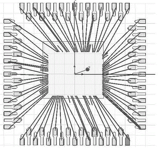
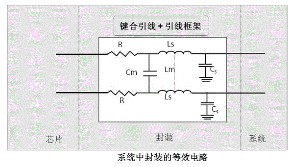
[0021] (1) Establish a three-dimensional physical model of the QFN package lead frame and bonding wire: give the physical parameters of different design dimensions of the lead frame and bonding wire suitable for the QFN package structure, including lead frame thickness, pin spacing, One or several design parameters such as the length of the bonding wire and the diameter of the bonding wire. Each parameter needs to give design dimensions of not less than four values. Then use three-dimensional electromagnetic field analysis software such as HFSS to establish a three-dimensional physical model, the effect of the model is as follo...


PUM


Abstract

The invention discloses a packaging parasitic parameter extraction method suitable for high speed IC-QFN packaging design utilization to extract electrical parameters of lead frames and bonding metal wires in a packaging structure. The parasitic parameter extraction method comprises the following steps of building QFN packaging three-dimensional physical models with different design sizes; utilizing an electromagnetic field full wave analytical method to extract scattering parameters of the QFN packaging structure in a certain frequency band range; building equivalent circuit models of the lead frames and the bonding wires; fitting out RLC lumped parameters of the equivalent circuit models through the extracted scattering parameters; summing up and sorting out an electric parameter data list of the lead frames and the bonding metal wires on different design conditions; building a mathematic model of physical parameter change related to the electric parameters through data analysis and the fitting algorithm; and finally extracting the parasitic parameters under any sizes. The parasitic parameter extraction method is simple and distinct in design thinking, and the electric parasitic parameters of the lead frames and the bonding metal wires with any sizes can be extracted directly without software simulation after the model is built, so that the flexibility of the packaging design is improved.

Description

technical field [0001] The invention relates to the technical field of semiconductor device packaging, more specifically the field of SPICE simulation and modeling of packaging structures. Background technique [0002] With the continuous improvement of the working speed of integrated circuits (ICs) and the development of electronic products towards miniaturization, portability, and ultra-thinness, packaging forms and assembly technologies with high density, high performance, and high reliability have been increasingly developed. more attention and research. [0003] In the prior art, the QFN package structure is a square flat no-lead semiconductor chip package structure. Because the QFN package does not have gull-wing leads like traditional SOIC and TSOP packages, the conductive path of the internal pins and pads is short, the self-inductance coefficient and the internal wiring resistance of the package are very low, so it can provide excellent electrical performance. ...

Claims


Application Information

Patent Timeline
IPC IPC(8): G06F17/50
Inventor 郑若彤蒋乐乐程玉华
Owner SHANGHAI RES INST OF MICROELECTRONICS SHRIME PEKING UNIV
Why Eureka
Try Eureka