n-type ldmos device and manufacturing method thereof

A manufacturing method and n-type technology, applied in the direction of semiconductor/solid-state device manufacturing, semiconductor devices, electrical components, etc., can solve the problems of affecting the electrical isolation of the device, limiting the application range of the device operating voltage, and reducing the punch-through voltage. The effect of design margins

Active Publication Date: 2015-06-03
SHANGHAI HUAHONG GRACE SEMICON MFG CORP
View PDF6 Cites 2 Cited by
  • Summary
  • Abstract
  • Description
  • Claims
  • Application Information

AI Technical Summary

Problems solved by technology

However, once the doping concentration of the deep n well 120 is reduced, the parasitic PNP transistor composed of the p-type body region 192, the deep n well 120, and the p-type substrate 100 will also be reduced due to the reduction of the doping concentration of the deep n well 132 as the base. Correspondingly, it will reduce its punch-through voltage, which will affect the electrical isolation of the device
Therefore, the above-mentioned n-type LDMOS device cannot simultaneously satisfy: improving the withstand voltage of the PN junction formed between the deep n well 120 and the p-type substrate 100, improving the parasitic PNP triode (by the p-type body region 192, the deep n well 120, the p type substrate 100) These two conflicting requirements of the punch-through voltage limit the application range of the device operating voltage

Method used


Image

  • n-type ldmos device and manufacturing method thereof
  • n-type ldmos device and manufacturing method thereof
  • n-type ldmos device and manufacturing method thereof

Examples


Embodiment Construction

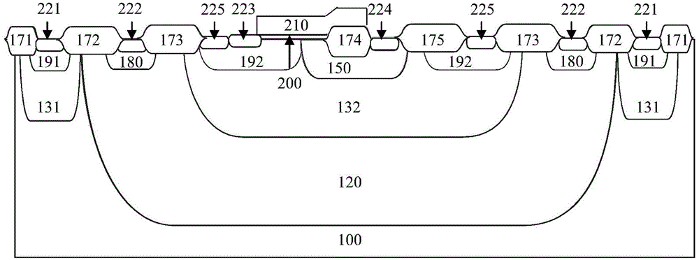
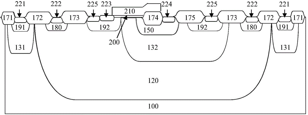
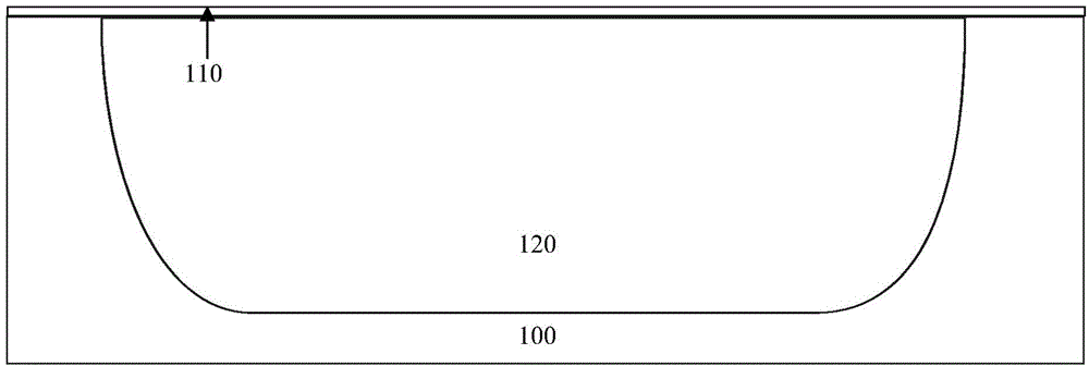
[0025] See Figure 5 , This is a schematic diagram of the cross-sectional structure of the n-type LDMOS device of the present application. The p-type lightly doped silicon substrate (or epitaxial layer) 100 has a lightly doped deep n-well 120 and a lightly doped p-well 131. The deep n-well 120 has the maximum junction depth. If viewed from a top view, the lightly doped p-well one 131 is a ring structure, surrounded by the outer side of the deep n-well 120, and the sides of the two are in contact with each other. The deep n-well 120 has a lightly doped p-well two 132, a heavily doped p-well two 192, and a heavily doped n-well two 180. The second heavily doped p-well 192 has a ring shape and is divided into two parts. The first part is directly in the deep n-well 120, and the second part is in the lightly doped p-well two 132. The first part of the second heavily doped p-well 192 and the side surface of the second lightly doped p-well 132 are in contact with each other. The r...


PUM


Abstract

The application discloses an n-type LDMOS device and a manufacturing method thereof. A p-type silicon substrate is internally provided with a deep n well and a low-doped p well I; the deep n well is internally provided with a low-doped p well II, a heavy-doped p well II and a heavy-doped n well II; the low-doped p well II is internally provided with a heavy-doped n well I; the heavy-doped p well II is internally provided with a source electrode and a body region extraction region; the heavy-doped n well I is internally provided with a drain electrode; the heavy-doped n well II is internally provided with a protection ring extraction region; parts of the heavy-doped n well II, the low-doped p well II and the heavy-doped n well I are provided with grid oxide layers; the grid oxide layers and a partial isolation structure IV adjacent to the grid oxide layers are provided with polysilicon grid electrodes; the low-doped p well I is internally provided with an annular heavy-doped p well I; the heavy-doped p well I is internally provided with a substrate extraction region; the surface of a silicon material is provided with multiple isolation structures. According to the n-type LDMOS device, the longitudinal punch-through voltage of a parasitic PNP triode in the n-type LDMOS device is improved, and the withstand voltage of a PN knot between the substrate and the deep n well is not changed.

Description

Technical field [0001] This application relates to a semiconductor device, in particular to an LDMOS (laterally diffused MOS transistor) device. Background technique [0002] See figure 1 , This is a schematic cross-sectional structure diagram of an existing n-type LDMOS device. The p-type lightly doped silicon substrate (or epitaxial layer) 100 has a lightly doped deep n-well 120 and a lightly doped p-well 131. A ring-shaped lightly doped p-well 131 surrounds the outer side of the deep n-well 120. The deep n-well 120 has a lightly doped p-well two 132 and a heavily doped n-well two 180, and a ring-shaped heavily doped n-well two 180 surrounds the lightly doped p-well two 132. The lightly doped p-well two 132 has a heavily doped p-well two 192 and a heavily doped n-well one 150, and a ring-shaped heavily doped p-well two 192 surrounds the heavily doped n-well one 150. A gate oxide layer 200 is provided on part of the heavily doped p-well two 192 and part of the heavily doped n...

Claims


Application Information

Patent Timeline
Patent Type & Authority Applications(China)
IPC IPC(8): H01L29/78H01L29/36H01L21/336
Inventor 李喆王黎陈瑜陈华伦
Owner SHANGHAI HUAHONG GRACE SEMICON MFG CORP
Why Eureka
Try Eureka