

Splicing and exposure method of sapphire substrate
A technology of sapphire substrate and exposure method, which is applied in the direction of microlithography exposure equipment, photolithography exposure device, etc., which can solve the problems of increasing the difficulty of operation, residual glue, and CD influence at the splicing of exposure field, etc.
- Summary
- Abstract
- Description
- Claims
- Application Information
AI Technical Summary
Problems solved by technology
Method used
Image

Examples
Embodiment 1
[0029] This embodiment provides a splicing exposure method for a patterned sapphire substrate, including:
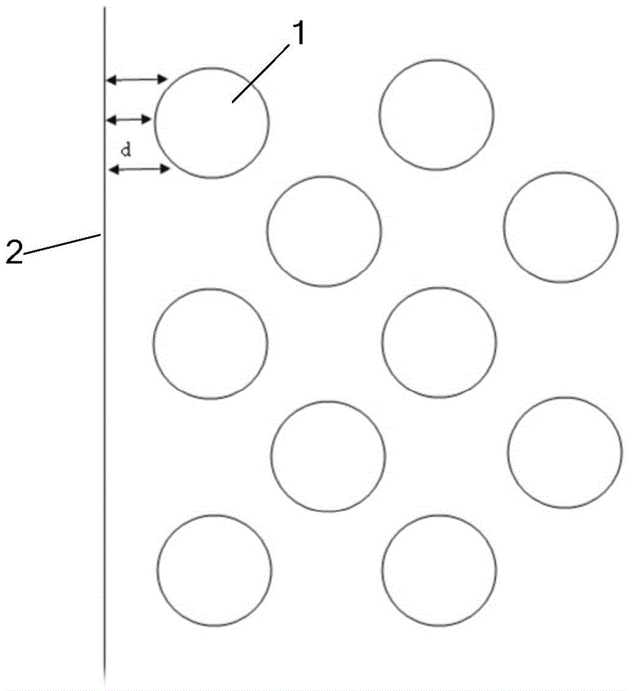
[0030] Before exposure, a mask pattern is supported on a mask according to the pattern to be supported on the surface of the patterned sapphire substrate. Composed of several unit graphics arranged on the light-transmitting area;
[0031] During exposure, all exposure areas on the surface of the sapphire substrate are exposed through the mask, and the exposure patterns of two adjacent exposure areas are spliced;
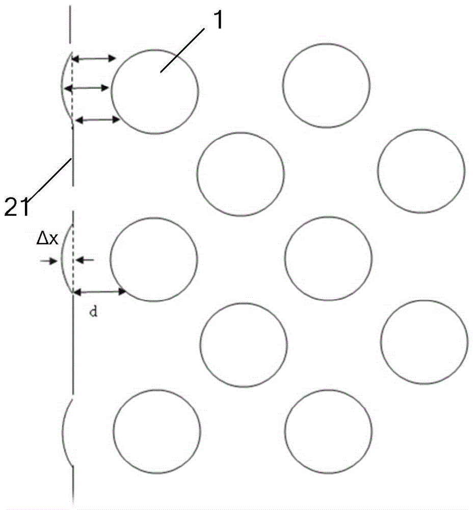
[0032] The boundary of the mask pattern is provided with a light-transmitting redundant portion outward, so as to enhance the exposure energy at the junction of two adjacent exposure areas.
[0033] In this embodiment, a mask is used to expose different exposure areas, and finally each exposure area is spliced to realize the exposure of the entire exposure field. Since splicing can be used to realize the exposure of the entire exposure field, there is no spe...
Embodiment 2
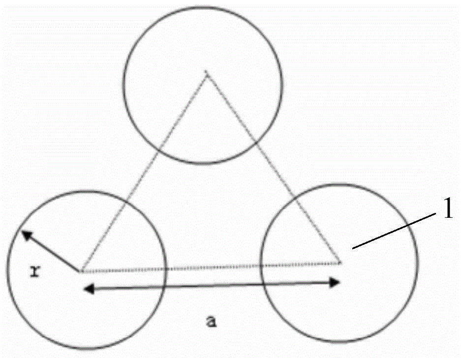
[0049] Please refer to Figure 8 to Figure 10 , the only difference between this embodiment and Embodiment 1 is that the unit figure is an equilateral triangle.
Embodiment 3
[0051] Please refer to Figure 8 to Figure 10 , the only difference between this embodiment and embodiment 1 is that the unit figure is a regular hexagon.
PUM
 Abstract
Description
Claims
Application Information