
FPGA chip and FPGA system

A chip and data selector technology, applied in the detection of faulty computer hardware, program control devices, etc., can solve the problems of occupying more FPGA chip pins, complex operation, and improving the complexity of FPGA system wiring.

Active Publication Date: 2015-06-10
HUAWEI TECH CO LTD
View PDF7 Cites 5 Cited by
  • Summary
  • Abstract
  • Description
  • Claims
  • Application Information

AI Technical Summary

Problems solved by technology

[0004] However, in order to realize the debugging of the FPGA system based on the JTAG (Joint Test Action Group) bus, in addition to the cascade connection between the FPGA chips through the DSP, it is also necessary to set the bypass in one FPGA chip. The controller is connected to each FPGA chip separately, so that more pins of the FPGA chip need to be occupied, which increases the complexity of the FPGA system connection
In addition, if adding or subtracting FPGA chips, it is necessary to re-layout the entire FPGA system to adjust the cascading relationship between FPGA chips, and the operation is complicated

Method used


Image

  • FPGA chip and FPGA system
  • FPGA chip and FPGA system
  • FPGA chip and FPGA system

Examples


Embodiment Construction

[0042] The FPGA chip and the FPGA system of the embodiments of the present invention will be described in detail below in conjunction with the accompanying drawings.

[0043] It should be clear that the described embodiments are only some of the embodiments of the present invention, not all of them. Based on the embodiments of the present invention, all other embodiments obtained by persons of ordinary skill in the art without making creative efforts belong to the protection scope of the present invention.

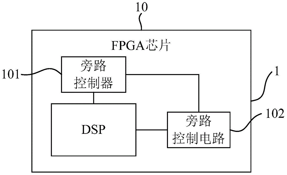
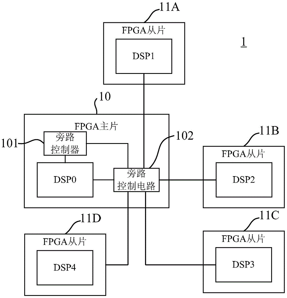
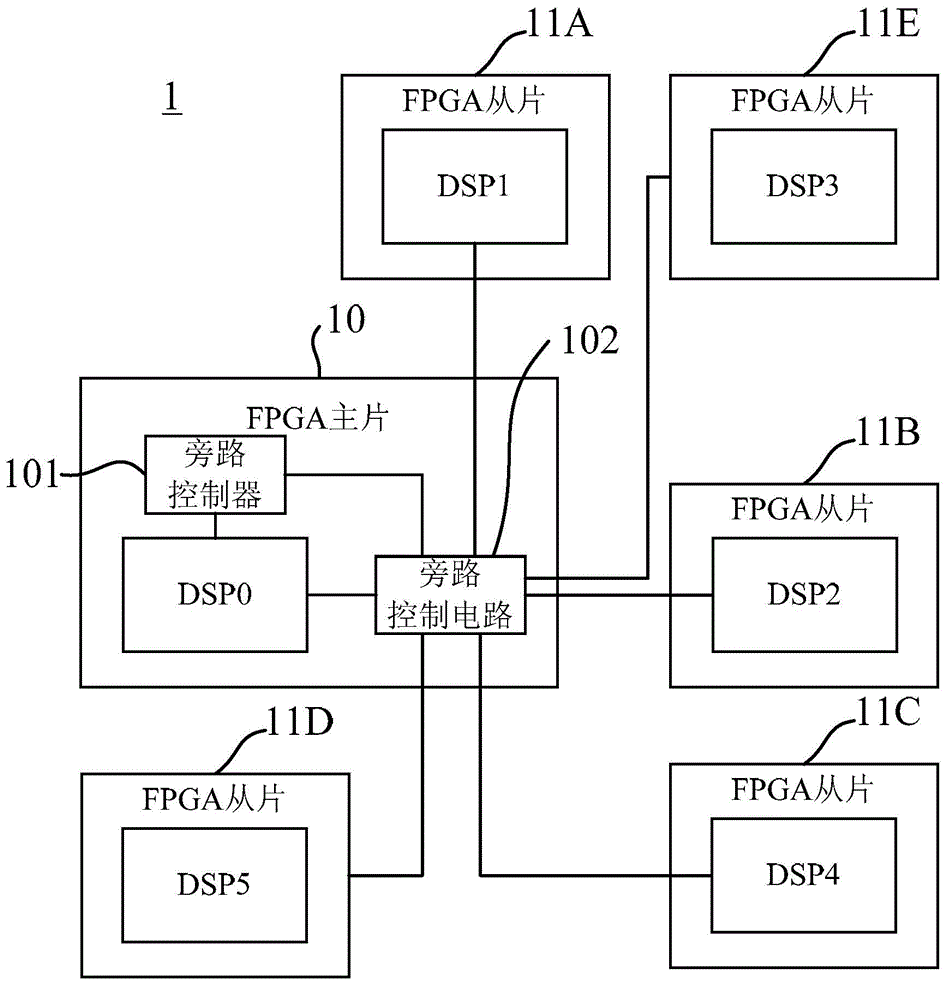
[0044] A FPGA chip 10, such as figure 1 As shown, the FPGA chip 10 is provided with a bypass controller 101 and a bypass control circuit 102 connected to the bypass controller 101;

[0045] In the FPGA system provided with the FPGA chip 10, the bypass control circuit 102 is connected to a plurality of DSPs, wherein each DSP is integrated in its own FPGA chip;

[0046] The bypass control circuit 102 is configured to perform data bypass on multiple DSPs according to a bypa...


PUM


Abstract

The invention discloses an FPGA chip and an FPGA system and belongs to the field of electrical apparatus elements. A bypass control circuit is integrated with an FPGA chip and is connected with another FPGA chip, so that the regulation of FPGA system layout can be simply and quickly achieved, and the usage amount of pins for the FPGA chips is also reduced. An FPGA chip is characterized in that a bypass controller and a bypass control circuit are arranged in the FPGA chip, wherein the bypass control circuit is connected with the bypass controller; in an FPGA system on which the FPGA chip is arranged, the bypass control circuit is connected with multiple digital signal processors; the bypass control circuit is used for carrying out data bypassing on the digital signal processors according to a bypassing instruction descended by the bypass controller.

Description

technical field [0001] The invention relates to the field of electrical components, in particular to an FPGA chip and an FPGA system. Background technique [0002] With the development of electronic technology, users have higher and higher requirements for the performance of product hardware, and the debugging of hardware in the process of product development is also becoming more and more complicated. [0003] In the prior art, product development is realized through the FPGA (Field Programmable Gate Array, Field-Programmable Gate Array) system. The FPGA system contains multiple FPGA chips, and one FPGA chip can be used as the main chip of the FPGA. Other FPGA chips act as FPGA slaves. A variety of components are integrated in the FPGA chip, such as the DSP (Digital Signal Processor) connected to the data selector. In multiple FPGA chips in the FPGA system, the DSP is set in a certain position and order. cascade. [0004] However, in order to realize the debugging of the...

Claims


Application Information

Patent Timeline
IPC IPC(8): G06F11/22G06F9/44
Inventor 潘葆梁
Owner HUAWEI TECH CO LTD
Learn More