Array substrate, manufacturing method thereof, and display device

An array substrate and active layer technology, applied in semiconductor/solid-state device manufacturing, electrical components, electric solid-state devices, etc., can solve the problems of pixel area reduction, storage capacitance reduction, process complexity, etc., to improve storage capacitance, The effect of increasing the storage capacitor and reducing the pixel area

Active Publication Date: 2017-10-13
BOE TECH GRP CO LTD
View PDF3 Cites 0 Cited by
  • Summary
  • Abstract
  • Description
  • Claims
  • Application Information

AI Technical Summary

Problems solved by technology

However, the continuous reduction of pixel area will inevitably lead to process complexity and reliability problems, as well as the continuous reduction of storage capacitance.

Method used


Image

  • Array substrate, manufacturing method thereof, and display device
  • Array substrate, manufacturing method thereof, and display device
  • Array substrate, manufacturing method thereof, and display device

Examples


Embodiment 1

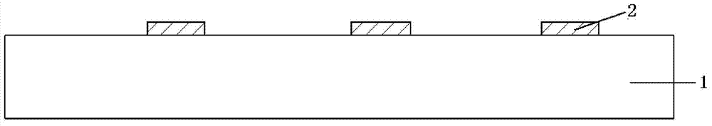
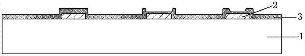
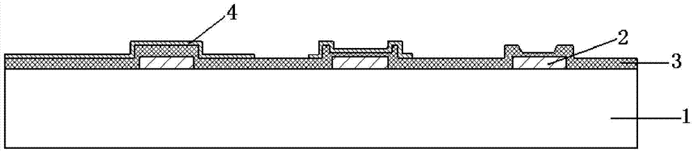
[0077] In order to explain the technical solution of the present invention more clearly, a specific embodiment 1 of the present invention will be described below in conjunction with the schematic cross-sectional view of the device structure formed in each step. In this embodiment, as Figure 8 As shown in the final product structure shown, the array substrate includes a thin film transistor area, a storage capacitor area, and a source and drain contact hole area, that is, the areas corresponding to the three gate electrode layers 2 from left to right in the figure. Of course, the array substrate also Other structures can be included, so I won't repeat them here. It should be understood that the structure shown here is exemplary, and other structural forms may be adopted according to the scope and spirit defined by the claims of the present invention. Such as Picture 9 As shown, the manufacturing method of this embodiment may specifically include the following steps:

[0078] S1:...


PUM


Abstract

An array substrate, a manufacturing method thereof and a display device are disclosed. The array substrate comprises a gate electrode layer (2), an active layer (4) and a source-drain electrode layer (6) that are disposed on a substrate (1). The substrate comprises a storage capacitance region thereon II. In the storage capacitance region II, projections of the gate electrode layer (2) and the active layer (4) on the substrate (1) are at least partially overlapped, and projections of the active layer (4) and the source-drain electrode layer (6) on the substrate (1) are at least partially overlapped. The array substrate can effectively increase the storage capacitance without increasing an area occupied by the storage capacitance region, which is advantageously to reduce a pixel area and increase PPI.

Description

Technical field [0001] The invention relates to the technical field of array substrate preparation, in particular to an array substrate, a manufacturing method thereof, and a display device. Background technique [0002] In recent years, display technology has been rapidly developed. For example, thin film transistor (Thin Film Transistor, TFT for short) technology has evolved from the original amorphous silicon thin film transistor to the current low-temperature polysilicon thin film transistor, metal oxide semiconductor thin film transistor, etc. The light-emitting technology has also developed from the original Liquid Crystal Display (LCD) technology to the current Organic Light-Emitting Diode (OLED) technology. [0003] Among them, oxide semiconductors have received increasing attention. Large-size oxide panels are currently in mass production and backplane performance enhancement. The mass-produced oxide backplanes are basically an Etch-Stopper Layer (ESL) structure. Since th...

Claims


Application Information

Patent Timeline
Patent Type & Authority Patents(China)
IPC IPC(8): H01L27/12H01L21/77H01L27/32
CPCH01L27/1255H01L27/1288
Inventor 刘晓娣王刚
Owner BOE TECH GRP CO LTD
Why Eureka
Try Eureka