Semiconductor laser, manufacturing method thereof and laser array

A production method and laser technology, applied in the field of optoelectronics, can solve the problems of high production cost, low production efficiency, high cost, etc., and achieve the effect that is conducive to uniform distribution of wavelength and light field, and favorable to precise control

Inactive Publication Date: 2015-06-10
CHINA INFOMRAITON CONSULTING & DESIGNING INST CO LTD
View PDF3 Cites 6 Cited by
  • Summary
  • Abstract
  • Description
  • Claims
  • Application Information

AI Technical Summary

Problems solved by technology

However, the method of electron beam exposure is to write the grating stripes one by one, which is very time-consuming and expensive to produce, which limits its practical application. If it is a multi-wavelength laser array, the production efficiency is lower and the cost is higher.

Method used


Image

  • Semiconductor laser, manufacturing method thereof and laser array
  • Semiconductor laser, manufacturing method thereof and laser array
  • Semiconductor laser, manufacturing method thereof and laser array

Examples


Embodiment

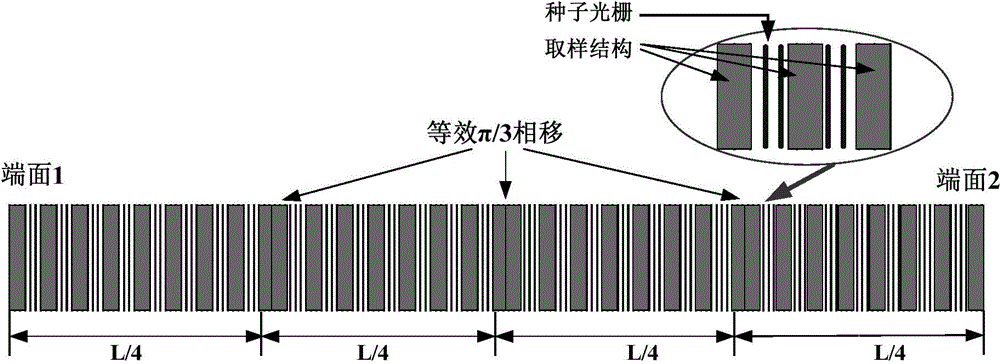
[0052] 1. Production of sampling grating

[0053] The DFB semiconductor laser in the present invention generally uses III-V compound semiconductor materials, such as GaAlAs / GaAs, InGaAs / InGaP, GaAsP / InGaP, InGaAsP / InP, InGaAsP / GaAsP, etc. At the same time, it can also be applied to various ternary compounds and quaternary compound semiconductor materials such as II-VI compound semiconductor materials and IV-VI compound semiconductor materials. In addition, the present invention can also be applied to aluminum-doped semiconductor materials (for example, AlGaInAs) for manufacturing semiconductor lasers without refrigeration and with good temperature characteristics. In order to reduce the influence of laser end face reflection, an anti-reflection coating can be coated on both end faces. The manufacturing key of laser of the present invention is to make sampling grating structure, and its concrete manufacturing method is:

[0054] (1) First design and manufacture a three-phase-...


PUM


Abstract

The invention discloses a semiconductor laser, a manufacturing method thereof and a multi-wavelength semiconductor laser array of the semiconductor laser. Three 2pi / 3 phase shifts are symmetrically arranged at a laser sampling grating, and the three 2pi / 3 phase shifts are symmetrically arranged at the 1 / 4, 1 / 2 and 3 / 4 parts of the length L of a laser cavity; the sampling grating is a Bragg grating, and moreover, the sampling grating is an equivalent phase shift grating.

Description

technical field [0001] The invention belongs to the technical field of optoelectronics, and relates to optical fiber communication, photon integration and other optoelectronic information processing. In particular, a three-phase-shifted DFB semiconductor laser based on reconstruction-equivalent chirp technology, a manufacturing method thereof, and a laser array. Background technique [0002] DFB (Distributed Feedback Laser), that is, distributed feedback laser semiconductor laser refers to a distributed feedback laser. Due to the built-in Bragg grating, it has good filtering characteristics and can filter out different wavelengths. High power, single longitudinal mode, narrow linewidth DFB semiconductor laser is the core light source of modern optical fiber communication. In order to improve the single-mode yield of DFB semiconductor lasers, a λ / 4 phase shift is usually introduced in the middle of the laser cavity. However, this λ / 4 phase shift makes the optical field distr...

Claims


Application Information

Patent Timeline
Patent Type & Authority Applications(China)
IPC IPC(8): H01S5/125H01S5/343H01S5/40
Inventor 卢林林魏贤虎易准俞力
Owner CHINA INFOMRAITON CONSULTING & DESIGNING INST CO LTD
Why Eureka
Try Eureka