808nm laser epitaxial wafer and preparation method thereof

An epitaxial wafer and laser technology, which is applied in the direction of lasers, laser components, semiconductor lasers, etc., can solve the problems of secondary epitaxial growth of high-quality materials, affecting the performance of lasers, and oxidation of aluminum-containing materials, so as to reduce space burning. Pore ​​effect, effect of improving crystal quality, improving output performance

Pending Publication Date: 2020-08-04
JIANGSU HUAXING LASER TECH CO LTD
View PDF0 Cites 0 Cited by
  • Summary
  • Abstract
  • Description
  • Claims
  • Application Information

AI Technical Summary

Problems solved by technology

At the same time, the choice of grating material and the introduction of Bragg microstructure have a great impact on the crystal quality of the secondary epitaxy and the carrier injection efficiency of the device, which in turn affects the working performance of the entire laser.
Generally speaking, GaAs-based materials usually use GaAs / AlGaAs materials to make Bragg reflector materials due to their lattice matching and large refractive index difference. come very difficult

Method used


Image

  • 808nm laser epitaxial wafer and preparation method thereof
  • 808nm laser epitaxial wafer and preparation method thereof
  • 808nm laser epitaxial wafer and preparation method thereof

Examples


Embodiment Construction

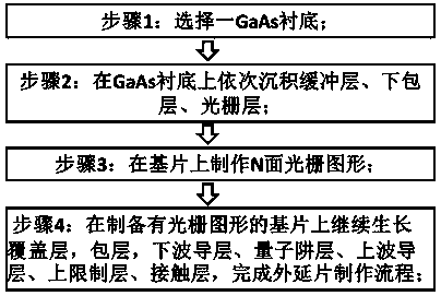
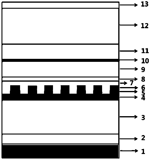
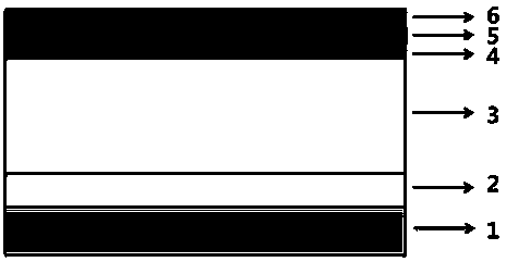
[0025] In order to make the object, technical solution and advantages of the present invention clearer, the present invention will be further described in detail below in conjunction with the accompanying drawings and specific embodiments. It should be understood that the specific embodiments described here are only used to explain the present invention, not to limit the present invention.

[0026] In the following text, many aspects of the invention will be better understood with reference to the accompanying drawings. Components in the figures are not necessarily drawn to scale. Instead, emphasis is placed on clearly illustrating the components of the invention. Furthermore, like reference numerals indicate corresponding parts throughout the several views of the drawings.

[0027] As used herein, the word "exemplary" or "illustrative" means serving as an example, instance, or illustration. Any implementation described herein as "exemplary" or "illustrative" is not necessa...


PUM

PropertyMeasurementUnit
thicknessaaaaaaaaaa
thicknessaaaaaaaaaa
thicknessaaaaaaaaaa

Abstract

The invention relates to the technical field of semiconductors, in particular to an 808nm laser epitaxial wafer and a preparation method thereof. The method is characterized by comprising the following steps of 1, selecting a GaAs substrate; 2, sequentially depositing a buffer layer, a lower limiting layer and a grating layer on the substrate; 3, preparing a grating pattern on the grating layer; and 4, continuously and sequentially growing a covering layer, a cladding layer, a lower waveguide layer, a quantum well layer, an upper waveguide layer, an upper limiting layer and a contact layer onthe grating layer on which the grating pattern is prepared to finish the preparation. The laser epitaxial wafer prepared by the method is low in wavelength drift coefficient and high in injection efficiency.

Description

technical field [0001] The invention relates to the technical field of semiconductors, in particular to an 808nm laser epitaxial wafer and a preparation method thereof. Background technique [0002] Since the advent of semiconductor lasers in the early 1960s, due to their performance advantages such as wide wavelength coverage, compact structure, high reliability and easy integration, they have been used in people's daily life, industrial and agricultural production, and national defense and military fields. be widely used. The performance of semiconductor lasers depends largely on the quality of semiconductor epitaxial wafers, so the preparation of high-quality epitaxial wafers is the key to the preparation of high-performance semiconductor lasers. The semiconductor laser working in the 808nm band is an indispensable pump source for the Nd:YAG laser. With the development of technology, compared with aluminum-containing materials, devices made of aluminum-free materials ha...

Claims


Application Information

Patent Timeline
Patent Type & Authority Applications(China)
IPC IPC(8): H01S5/026H01S5/34
CPCH01S5/0268H01S5/3401H01S2304/00
Inventor 罗帅季海铭徐鹏飞王岩王俊徐智鹏
Owner JIANGSU HUAXING LASER TECH CO LTD
Why Eureka
Try Eureka