

Method for manufacturing zinc-doped ultra shallow junction on surface of semiconductor substrate
A substrate surface, semiconductor technology, used in semiconductor/solid-state device manufacturing, electrical components, circuits, etc., can solve problems such as junction leakage, and achieve the effects of controllable junction depth, good growth thickness uniformity, and small lattice damage
- Summary
- Abstract
- Description
- Claims
- Application Information
AI Technical Summary
Problems solved by technology
Method used
Image

Examples
Embodiment Construction
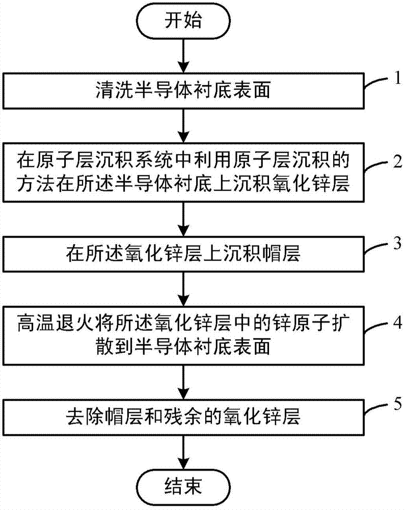
[0032] In order to make the object, technical solution and advantages of the present invention clearer, the present invention will be described in further detail below in conjunction with specific embodiments and with reference to the accompanying drawings.
[0033] The method for preparing a zinc-doped ultra-shallow junction on the surface of a semiconductor substrate provided by the present invention is to deposit a zinc oxide layer on the semiconductor substrate, deposit a cap layer on the zinc oxide layer, and then diffuse zinc to the semiconductor substrate by annealing. In the bottom, the cap layer is removed by etching or etching to form a zinc-doped ultra-shallow junction.
[0034] Such as figure 1 as shown, figure 1 It is a flowchart of a method for forming a zinc-doped ultra-shallow junction on a semiconductor substrate according to an embodiment of the present invention. The method is to prepare zinc on the surface of the semiconductor substrate by diffusing zinc i...
PUM
| Property | Measurement | Unit |
|---|---|---|
| thickness | aaaaa | aaaaa |
| thickness | aaaaa | aaaaa |
| thickness | aaaaa | aaaaa |
Abstract
Description
Claims
Application Information