A kind of cadmium telluride thin film solar cell module and preparation method thereof
A solar cell, cadmium telluride technology, applied in electrical components, circuits, photovoltaic power generation, etc., can solve the problems of difficult control, complex preparation of composite layers, etc., and achieve the effects of prolonging service life, efficiency attenuation, and good stability
- Summary
- Abstract
- Description
- Claims
- Application Information
AI Technical Summary
Problems solved by technology
Method used
Image
Examples
preparation example Construction
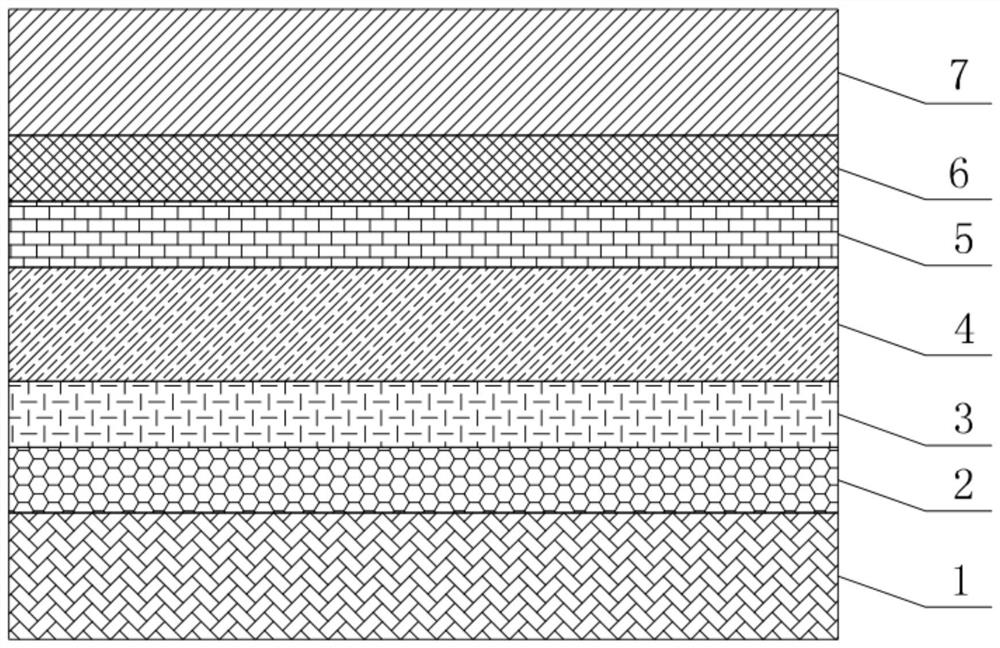
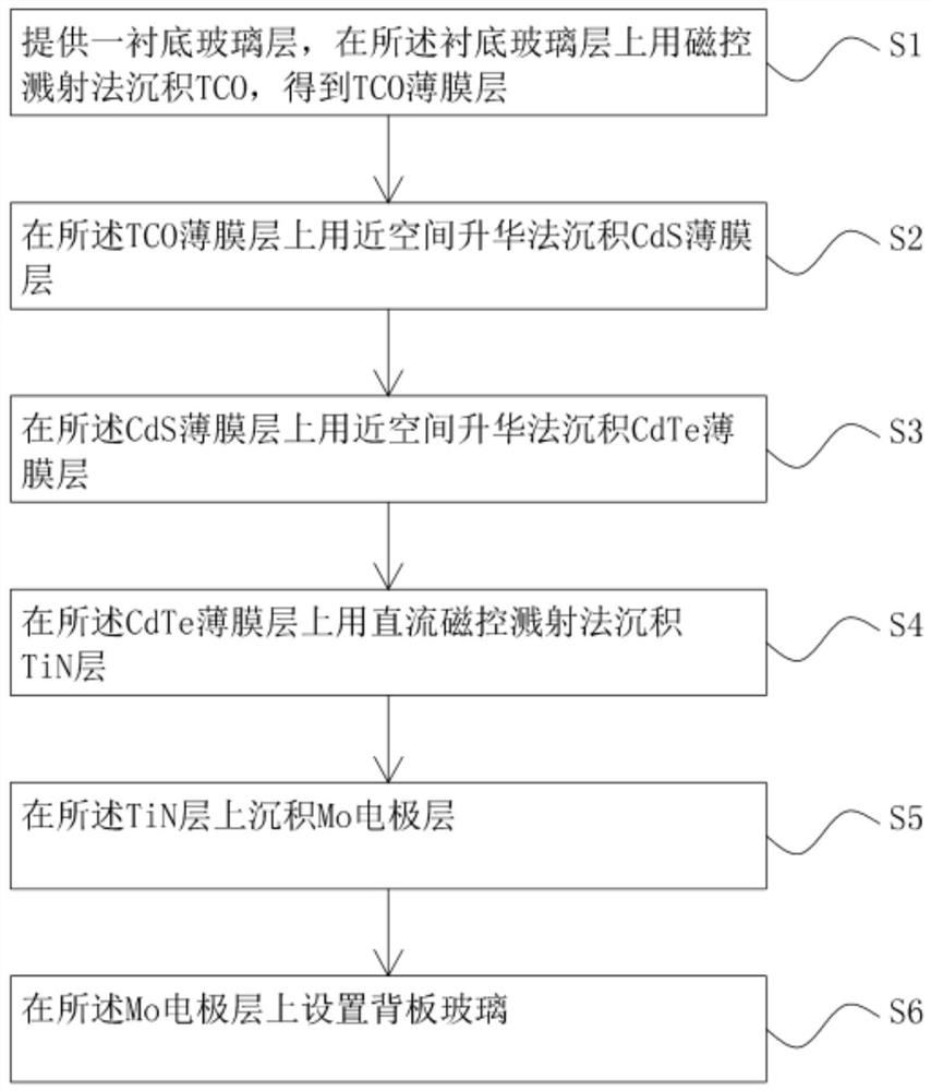
[0034] A method for preparing a cadmium telluride thin film solar cell assembly, comprising the steps of:
[0035] S1 provides a substrate glass layer 1 on which TCO is deposited by magnetron sputtering to obtain a TCO thin film layer 2;
[0036] S2 depositing a CdS thin film layer 3 on the TCO thin film layer 2 by a close-space sublimation method;
[0037] S3 depositing a CdTe thin film layer 4 on the CdS thin film layer 3 by a close space sublimation method;
[0038] S4 deposits a TiN layer on the CdTe film layer 4 by DC magnetron sputtering;
[0039] S5 deposits a Mo electrode layer 6 on the TiN layer;
[0040] S6 disposing a backplane glass layer 7 on the Mo electrode layer 6 .
[0041] Preferably, in the step S4, the TiN layer is coated with a 150 mm circular titanium target in a mixed atmosphere of argon gas with a purity of 99.99% and a nitrogen gas with a purity of 99.95%.
[0042] More preferably, the total pressure of the mixed gas of argon and nitrogen is 0.8pa,...
Embodiment 1
[0045] A substrate glass layer 1 is provided, and TCO is deposited by magnetron sputtering on the substrate glass layer 1 to obtain a TCO film layer 2 with a thickness of 300 nm; CdS, to obtain a CdS film layer 3 with a thickness of 50nm; on the CdS film layer 3, deposit CdTe with a close-space sublimation method to obtain a CdTe film layer 4 with a thickness of 2um; TiN is deposited by sputtering to obtain a TiN layer with a thickness of 50 nm; a Mo electrode layer 6 is deposited on the TiN layer; and a back glass layer 7 is arranged on the Mo electrode layer 6 .
Embodiment 2
[0047] A substrate glass layer 1 is provided, and TCO is deposited by magnetron sputtering on the substrate glass layer 1 to obtain a TCO film layer 2 with a thickness of 400 nm; CdS, to obtain a CdS film layer 3 with a thickness of 120nm; on the CdS film layer 3, deposit CdTe with a close-space sublimation method to obtain a CdTe film layer 4 with a thickness of 4um; TiN is deposited by sputtering to obtain a TiN layer with a thickness of 150 nm; a Mo electrode layer 6 is deposited on the TiN layer; and a backplane glass layer 7 is arranged on the Mo electrode layer 6 .
PUM
| Property | Measurement | Unit |
|---|---|---|
| thickness | aaaaa | aaaaa |
| thickness | aaaaa | aaaaa |
| thickness | aaaaa | aaaaa |
Abstract
Description
Claims
Application Information


