A kind of flip-chip LED chip and preparation method thereof

A LED chip and flip-chip technology, which is applied in the direction of electrical components, circuits, semiconductor devices, etc., can solve the problems of complicated packaging process and high cost, and achieve the effect of reducing production cost and simplifying the packaging process

Active Publication Date: 2018-04-17
LATTICE POWER (JIANGXI) CORP
View PDF4 Cites 2 Cited by
  • Summary
  • Abstract
  • Description
  • Claims
  • Application Information

AI Technical Summary

Problems solved by technology

However, when packaging is used, first coat a layer of solder paste on the substrate, then place the chip upside down on the substrate, and fix it by eutectic soldering. Such a packaging process is complicated and expensive.

Method used


Image

  • A kind of flip-chip LED chip and preparation method thereof
  • A kind of flip-chip LED chip and preparation method thereof
  • A kind of flip-chip LED chip and preparation method thereof

Examples


Embodiment Construction

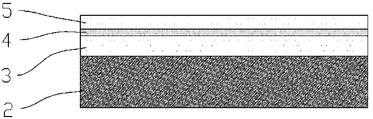
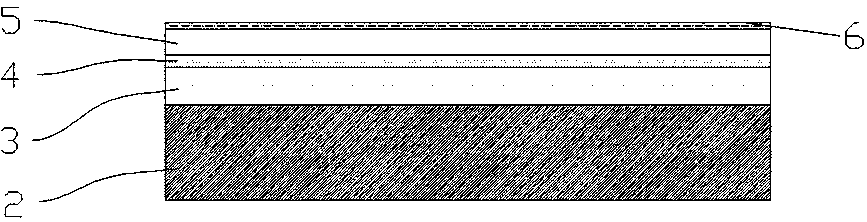
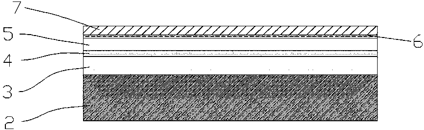
[0020] The present invention proposes a flip-chip LED chip, including a sapphire substrate, an InGaAlN multilayer structure formed on the sapphire substrate, and the InGaAlN multilayer structure includes an N-type GaN layer, a multi-quantum well layer and a P type GaN layer, a reflective layer formed on the P-type GaN layer, a metal protective layer deposited on the surface of the reflective layer, etched in a part of the metal protective layer to expose the N electrode hole formed by the N-type GaN layer. The passivation layer formed by the partial area of ​​the surface of the protective layer and the side wall of the N electrode hole, the N electrode formed by depositing metal in the N electrode hole and connecting multiple N electrode holes, the metal protection not covered by the passivation layer The P electrode formed on the layer also includes a solder paste layer formed on the N electrode and the P electrode, and a metal barrier layer is formed around the solder paste l...


PUM


Abstract

The present invention is a flip-chip LED chip and its preparation method, comprising a sapphire substrate, an InGaAlN multilayer structure formed on the sapphire substrate, and the InGaAlN multilayer structure includes an N-type GaN layer and multiple quantum wells from bottom to top layer and a P-type GaN layer, a reflective layer formed on the P-type GaN layer, a metal protective layer deposited on the surface of the reflective layer, and a part of the metal protective layer is etched to expose the N formed by the N-type GaN layer. Electrode holes, the passivation layer formed on the part of the surface of the metal protective layer and the side walls of the N electrode holes, the N electrodes formed by depositing metal in the N electrode holes and connecting multiple N electrode holes, The P electrode formed on the metal protection layer covered by the passivation layer is characterized in that the flip-chip LED chip also includes a solder paste layer formed on the N electrode and the P electrode, and a metal barrier is formed around the solder paste layer. Floor.

Description

technical field [0001] The invention relates to light emitting diode technology, in particular to sapphire substrate LED flip-chip technology. Background technique [0002] At present, high-power and high-brightness LEDs have become the focus of the development of the LED industry and are widely used in indoor and outdoor lighting. Considering that the conductivity of the P-GaN layer of traditional positive-mounted sapphire substrate high-power chips is not high, it is necessary to deposit a semi-transparent Ni / Au conductive layer on the upper surface of the P-type layer to make the current more evenly distributed. The current diffusion layer will absorb Part of the light reduces the light efficiency, and the low thermal conductivity of sapphire leads to high thermal resistance of the chip. In order to overcome the above disadvantages, a flip chip has been proposed. In this way, the light emitted by the active area is taken out through the transparent sapphire substrate, w...

Claims


Application Information

Patent Timeline
Patent Type & Authority Patents(China)
IPC IPC(8): H01L33/62H01L33/00
Inventor 彭翔赵汉民张璟金力傅建华
Owner LATTICE POWER (JIANGXI) CORP
Why Eureka
Try Eureka