Waveform calibration using built in self test mechanism

A harmonic component, constant frequency technology, applied in the field of waveform shape optimization, can solve problems such as limiting the scope of the design team, shortening the design cycle, etc., to achieve the effect of consumption optimization

CN104734787AActive Publication Date: 2015-06-24TEXAS INSTR INC
6 Cites 12 Cited by

Patent Information

Authority / Receiving Office
CN · China
Current Assignee / Owner
Publication Date
2015-06-24

Smart Images

  • Figure 1
    Figure 1
  • Figure 2
    Figure 2
  • Figure 3
    Figure 3
Patent Text Reader

Abstract

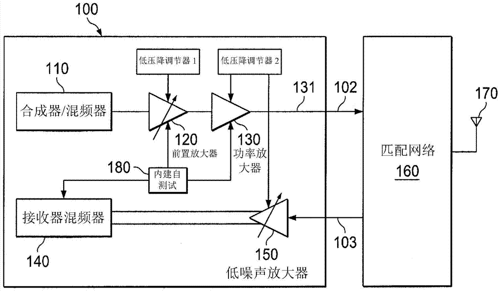
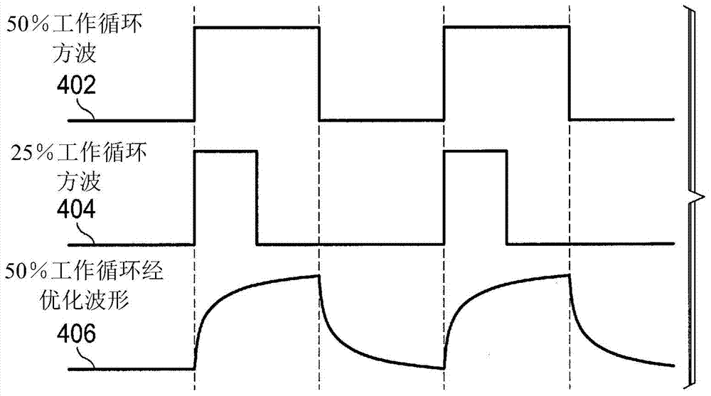
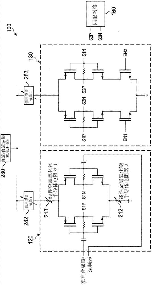
A system on a chip (SoC) includes a transceiver comprising a transmitter having a power amplifier and a receiver having a signal buffer. At least one of the transmitter and receiver has a configurable portion that can be configured to produce a range of waveforms (both in waveshape as well as duty cycle). A low cost built in self test (BIST) logic is coupled to the transceiver. The BIST logic is operable to calibrate the configurable portion of the transceiver to produce a waveform that has a selected harmonic component that has an amplitude that is less than a threshold value. Current consumed by the transceiver may be dynamically reduced by selecting an optimized waveform that has low harmonic components.
Need to check novelty before this filing date? Find Prior Art

Description

technical field

[0001] Embodiments of the present invention relate generally to transceivers for radio frequency transmission, and in particular to optimization of the waveform shape of high speed clock signals within transceivers to reduce power consumption. Background technique

[0002] System-on-Chip (SoC) is a concept that has existed for a long time; the basic approach is to integrate more and more functionality into a given device. This integration can take the form of hardware or solution software. Many SoC designs pair one or more microprocessor cores with various peripheral devices and memory circuits.

[0003] A radio frequency (RF) transceiver may be included within the SoC and may include a fully integrated CMOS low noise amplifier (LNA) and power amplifier (PA). A differential circuit is usually chosen to reduce the effect of ground noise in the LNA circuit and to double the output power level of the PA at the same supply voltage.

[0004] The Bluetooth stand...

Examples

example

[0092] Figure 7 is a block diagram of an example SoC 700 including a digital radio 730 including a Bluetooth transceiver 732 . Transceiver 732 includes adjustable amplifiers and buffers that may be calibrated to reduce current usage as described in more detail above. Calibration may be performed by writing control words into radio control registers 734 under the control of BIST module 780 . Demodulation logic 736 may contain a digital signal processor that may be configured to perform FFT calculations on digital data received via receiver 720 during the calibration process. Software applications stored in memory 704 and executed by processor 702 may control and configure the digital radio as required by applications executing thereon. The general operation of Bluetooth radios is known, and therefore it will not be described in further detail herein. Matching network 760 is similar to the matching network described earlier.

[0093] The BIST module 780 can be configured to...