Circuit board processing method and device

A processing method and processing equipment technology, applied in printed circuit, multi-layer circuit manufacturing, printed circuit manufacturing, etc., can solve the hidden danger of voltage resistance and affect the safety of large PCB work, etc.

Active Publication Date: 2015-06-24
SHENNAN CIRCUITS
View PDF8 Cites 1 Cited by
  • Summary
  • Abstract
  • Description
  • Claims
  • Application Information

AI Technical Summary

Problems solved by technology

[0003] In order to reduce the thickness of the PCB, most manufacturers mainly achieve this by reducing the number of prepregs used in the PCB. In practice, it is found that the dielectric thickness of the PCB can be reduced by reducing the number of prepregs used. Becau

Method used


Image

  • Circuit board processing method and device
  • Circuit board processing method and device
  • Circuit board processing method and device

Examples


Embodiment Construction

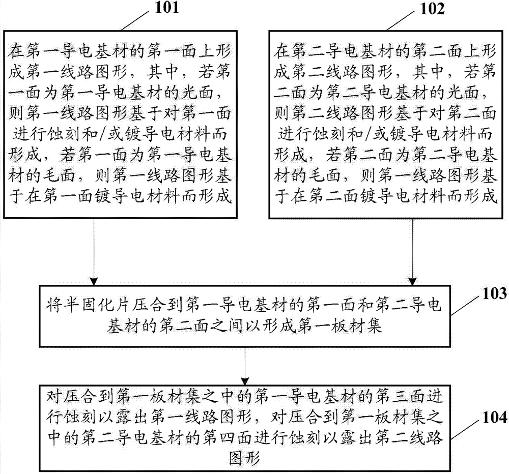
[0041] Embodiments of the present invention provide a circuit board processing method and circuit board processing equipment, so as to improve the withstand voltage performance of the PCB on the premise of controlling the thickness of the prepreg in the PCB as much as possible.

[0042] The technical solutions in the embodiments of the present invention will be clearly and completely described below with reference to the accompanying drawings in the embodiments of the present invention. Obviously, the described embodiments are only a part of the embodiments of the present invention, but not all of the embodiments. Based on the embodiments of the present invention, all other embodiments obtained by those of ordinary skill in the art without creative efforts shall fall within the protection scope of the present invention.

[0043] The terms "first", "second", "third", "fourth", etc. (if any) in the description and claims of the present invention and the above-mentioned drawings a...


PUM


Abstract

The embodiment of the invention discloses a circuit board processing method and device. The circuit board processing method comprises the steps that a first line pattern is formed on a first face of a first conductive substrate, and if the first face is a rough face of the first conductive substrate, the first line pattern is formed based on the mode that the first face is plated with a conductive material; a second line pattern is formed on a second face of a second conducive substrate, and if the second face is a rough face of the second conductive substrate, the second line pattern is formed based on the mode that the second face is plated with the conductive material; a prepreg is arranged between the first face of the first conductive substrate and the second face of the second conductive substrate through press fit, so that a first board material set is formed; a third face of the first conductive substrate in the first board material set is etched so that the first line pattern can be exposed, and a fourth face of the second conductive substrate in the first board set is etched so that the second line pattern can be formed. According to the scheme, on the premise that the thickness of the prepreg in the PCB is controlled to the greatest extent, the voltage resistance of the PCB is improved.

Description

technical field [0001] The invention relates to the technical field of circuit board processing and manufacturing, in particular to a circuit board processing method and circuit board processing equipment. Background technique [0002] As electronic products require more and more functions, the number of layers of printed circuit boards (PCB, Printed circuit board) is also required to increase, but the higher the number of PCB layers, the thicker its thickness, and the required assembly space. The larger it is, and this is contrary to the requirements of light, thin, short, and small electronic products. [0003] In order to reduce the thickness of the PCB, most manufacturers mainly achieve this by reducing the number of prepregs used in the PCB. In practice, it has been found that the dielectric thickness of the PCB can be reduced by reducing the number of prepregs used. Because of the existence of lines, if the actual PCB The effective dielectric thickness is too low. For...

Claims


Application Information

Patent Timeline
IPC IPC(8): H05K3/46
CPCH05K3/4611
Inventor 刘宝林张静峰
Owner SHENNAN CIRCUITS
Why Eureka
Try Eureka