Semiconductor device and forming method thereof

A semiconductor and device technology, applied in the field of semiconductor devices and their formation, can solve problems such as unstable performance of pressure sensors, and achieve the effects of good contact interface quality, stable performance and low contact resistance

Active Publication Date: 2015-07-01
SEMICON MFG INT (SHANGHAI) CORP +1
View PDF7 Cites 9 Cited by
  • Summary
  • Abstract
  • Description
  • Claims
  • Application Information

AI Technical Summary

Problems solved by technology

[0005] However, the performance of e

Method used


Image

  • Semiconductor device and forming method thereof
  • Semiconductor device and forming method thereof
  • Semiconductor device and forming method thereof

Examples


Embodiment Construction

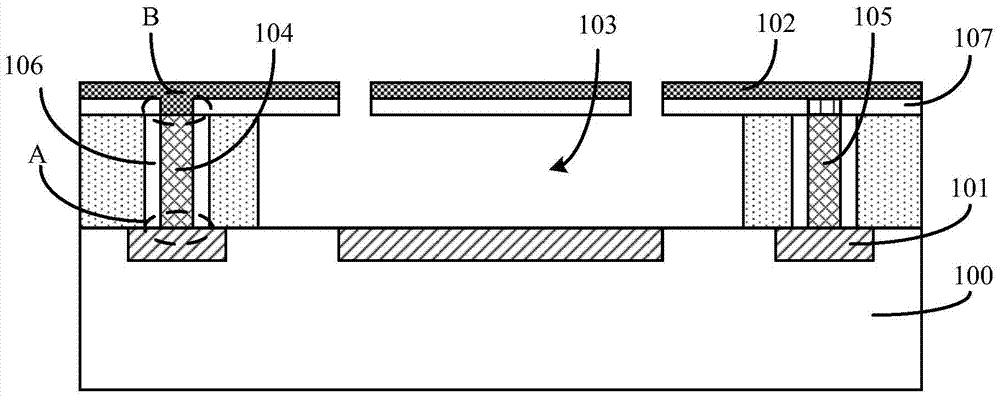
[0032] As mentioned in the background art, the performance of existing pressure sensors is not stable.

[0033] figure 1 It is a schematic cross-sectional structure diagram of a sensor, including: a substrate 100; a first electrode layer 101 located on the surface of the substrate 100; a second electrode layer 102 located on the surface of the substrate 100 and the first electrode layer 101, the first electrode There is a cavity 103 between the layer 101 and the second electrode layer 102; there is a first conductive plug 104 and a second conductive plug 105 between the first electrode layer 101 and the second electrode layer 102, and the second conductive The plug 105 is electrically isolated from the second electrode layer 102 by an insulating layer, while the first conductive plug 104 and the first electrode layer 101 at the bottom of the second conductive plug 105 are not connected; the first conductive plug 104 and The sidewall surface of the second conductive plug 105 i...


PUM

PropertyMeasurementUnit
Thicknessaaaaaaaaaa
Thicknessaaaaaaaaaa

Abstract

The invention discloses a semiconductor device and a forming method thereof. The forming method of the semiconductor device comprises the following steps: providing a substrate, wherein a first conductive layer is arranged on the surface of the substrate, a sacrificial layer is arranged on the surface of the first conductive layer, a mask layer is arranged on the surface of the sacrificial layer, and the mask layer is exposed on part of the surface of the sacrificial layer; taking the mask layer as a mask, etching the sacrificial layer until the first conductive layer is exposed, and forming a first opening and a second opening in the sacrificial layer; forming conductive films on the surface of the mask layer and on the side walls and bottom surfaces of the first opening and the second opening; forming dielectric layers full of the first opening and the second opening on the surfaces of the conductive films; removing part of conductive films on the surface of the mask layer so as to pattern the conductive films after the dielectric layers are formed, forming a first plug in the first opening, forming a second plug in the second opening, and forming a second conductive layer on the surface of the mask layer, wherein the second plug and the second conductive layer are in electrical open circuit; and electrically connecting the second conductive layer with the first plug. Therefore, the performance of the formed semiconductor device is stable and good.

Description

technical field [0001] The invention relates to the technical field of semiconductor manufacturing, in particular to a semiconductor device and a forming method thereof. Background technique [0002] Micro-Electro Mechanical System (MEMS for short) is an integrated device that acquires information, processes information and performs operations. Sensors in MEMS can receive external information such as pressure, position, velocity, acceleration, magnetic field, temperature or humidity, and convert the obtained external information into electrical signals for processing in MEMS. A pressure sensor is a conversion device that converts pressure signals into electrical signals. [0003] A capacitive pressure sensor is one of the existing pressure sensors. A capacitive pressure sensor in the prior art includes: a substrate; a first electrode layer located on the surface of the substrate; a second electrode layer located on the surface of the substrate and the first electrode layer....

Claims


Application Information

Patent Timeline
IPC IPC(8): B81C1/00B81B3/00B81B7/00
Inventor 伏广才张先明刘庆鹏
Owner SEMICON MFG INT (SHANGHAI) CORP
Why Eureka
Try Eureka