

PVD preparation process for adjusting TiW membrane stress
A technology of preparation process and film stress, which is applied in the direction of metal material coating process, ion implantation plating, coating, etc., can solve problems such as changes in the density of TiW films, improve stability and service life, and meet stress requirements Effect
- Summary
- Abstract
- Description
- Claims
- Application Information
AI Technical Summary
Problems solved by technology
Method used
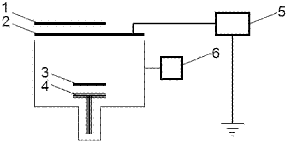
Image

Examples
preparation example Construction
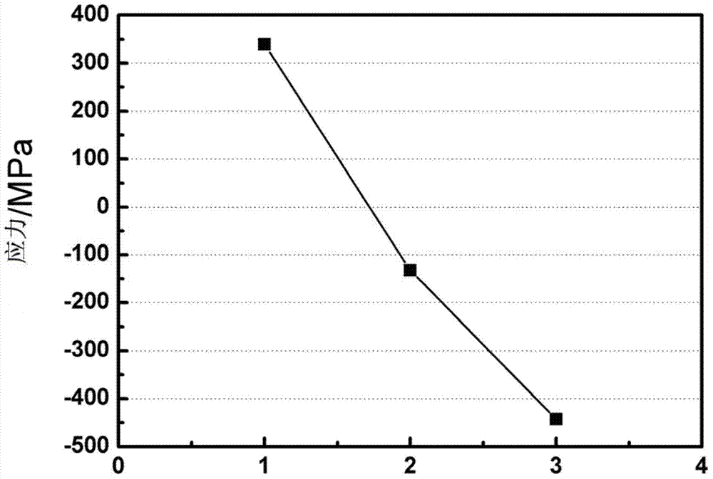
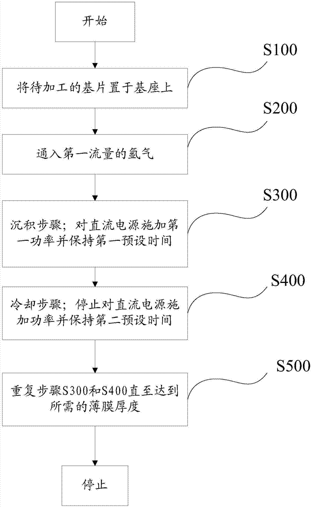
[0033] The key process parameters in the preparation process of the present invention are deposition time and cooling time, namely the first preset time and the second preset time. Generally, the first preset time is 5s to 30s, and the second preset time is 60s to 360s. By setting different deposition time and cooling time, the stress of TiW film can be adjusted to meet different stress requirements.
[0034] It should be noted that before applying power to the DC power supply, a step of igniting the DC power supply is also included. Generally, the ignition time of the DC power supply is 2s.
[0035] Preferably, as an implementable manner, the following process parameters such as the flow rate of argon gas, the deposition pressure and the power of the DC power supply are kept constant throughout the entire preparation process. This can ensure that the deposition rate and density of the prepared TiW thin film remain basically unchanged, thereby improving the stability and ser...
PUM
| Property | Measurement | Unit |
|---|---|---|
| thickness | aaaaa | aaaaa |
Abstract
Description
Claims
Application Information