Manufacturing method of display substrate, display substrate and display device

A manufacturing method and display substrate technology, which are applied to the display substrate manufacturing method, display substrate and display device fields, can solve the problems of brightness, color gamut reduction, aperture ratio reduction, energy consumption increase, etc., to improve the display contrast and improve the picture quality, the effect of reducing reflectivity

Active Publication Date: 2015-07-01
BOE TECH GRP CO LTD
View PDF5 Cites 28 Cited by
  • Summary
  • Abstract
  • Description
  • Claims
  • Application Information

AI Technical Summary

Problems solved by technology

[0003] In the prior art LCD display devices, the array substrate and the filter substrate are pasted together through a box-forming process, and there will be a certain deviation between the patterns corresponding to the array substrate and the filter substrate when the box is formed, and the deviation will be

Method used


Image

  • Manufacturing method of display substrate, display substrate and display device
  • Manufacturing method of display substrate, display substrate and display device
  • Manufacturing method of display substrate, display substrate and display device

Examples


Embodiment Construction

[0036] In order to make the technical problems, technical solutions and advantages to be solved by the embodiments of the present invention clearer, the following will describe in detail with reference to the drawings and specific embodiments.

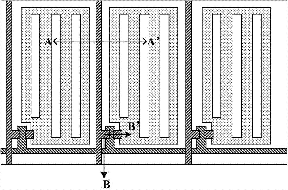
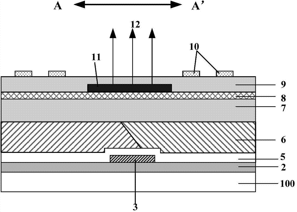
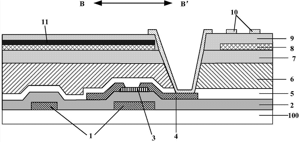
[0037] An embodiment of the present invention provides a method for manufacturing a display substrate, wherein the method includes a step of forming a black matrix, and the step of forming a black matrix is ​​as follows: Figure 5 shown, including:

[0038] Step 51, forming a metal pattern for making the black matrix, the metal pattern adopts an amphoteric metal or an amphoteric metal alloy;

[0039] Step 52 , treating the metal pattern with an alkaline solution to form the black matrix with a rough surface.

[0040] In the embodiment of the present invention, the amphoteric metal or amphoteric metal alloy material is used to make the black matrix, and the surface of the metal black matrix is ​​treated with an alkaline solution. Since...


PUM


Abstract

The invention provides a manufacturing method of a display substrate, the display substrate and a display device. The method comprises the step of forming a black matrix; when forming the black matrix, a metal graph for manufacturing the black matrix is formed, wherein the metal graph is prepared from metalloid or metalloid alloy; the metal graph is treated through an alkaline solution so as to form the black matrix with rough surface. According to the method, the metal black matrix with the rough surface can be formed, so that the reflecting rate of a metal material can be reduced; in addition, the reflecting rate of the display panel to the outside light can be reduced; the display contrast ratio is increased, and the image quality is improved.

Description

technical field [0001] The invention relates to the field of liquid crystal display, in particular to a manufacturing method of a display substrate, a display substrate and a display device. Background technique [0002] Display devices such as liquid crystal display devices LCD and organic electroluminescent devices OLED have become a necessity in people's lives and are quietly changing people's lives. People's requirements for the resolution, color gamut, and brightness of display devices are also increasing. High, recently companies have developed products with a pixel density (PPI) of 500 or even 600PPI. [0003] In the prior art LCD display devices, the array substrate and the filter substrate are pasted together through a box-forming process. There will be a certain deviation between the patterns corresponding to the array substrate and the filter substrate when the box is formed, and the deviation will be This leads to problems such as a decrease in the aperture rati...

Claims


Application Information

Patent Timeline
IPC IPC(8): G02F1/1335G02F1/1333H01L27/12G03F7/00
CPCG02F1/133514G02F1/133516G02F1/136209G02F1/13439H01L27/1225G02F1/136222G02F1/133512H01L27/124H01L27/1262H01L29/7869G02F1/136286G02F1/136295
Inventor 张锋曹占锋姚琪
Owner BOE TECH GRP CO LTD
Why Eureka
Try Eureka