Substrate etching method

A technology of substrate and etching gas, applied in the field of microelectronics, can solve problems such as process failure, critical dimension shrinkage at the bottom of the side wall, and etching interruption.

CN104752197AActive Publication Date: 2015-07-01BEIJING NAURA MICROELECTRONICS EQUIP CO LTD
5 Cites 1 Cited by

Patent Information

Authority / Receiving Office
CN · China
Patent Type
Applications(China)
Current Assignee / Owner
Publication Date
2015-07-01

Smart Images

  • Figure 1
    Figure 1
  • Figure 2
    Figure 2
  • Figure 3
    Figure 3
Patent Text Reader

Abstract

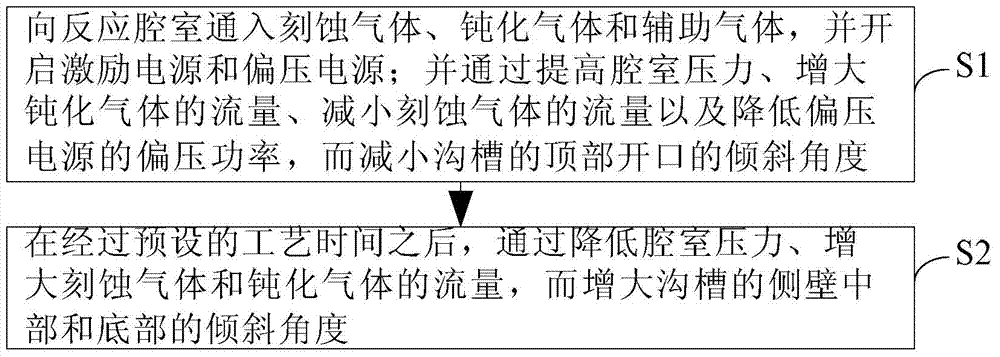
The invention provides a substrate etching method. The method comprises the steps that S1) etching gas, passivation gas and auxiliary gas are input into a reaction chamber, an excitation power supply and a bias power supply are started, and the inclination of an opening at the top of a groove is reduced by increasing the pressure of the chamber and the flow of the passivation gas and reducing the flow of the etching gas and the bias power of the bias power supply; and S2) after a preset technical time, the inclination of the middle and bottom portions of the sidewall of the groove is increased by reducing the pressure of the chamber and increasing the flow of the etching gas and the passivation gas. The etching gas comprises fluorine and sulfur composite gas, the passivation gas includes oxygen, and the auxiliary gas comprises inert gas. According to the substrate etching method, an ideal substrate appearance that the opening at the top of the groove inclines to form a V shape, the middle and bottom portions of the sidewall are steep, and the bottom surface is smooth can be obtained.
Need to check novelty before this filing date? Find Prior Art

Description

technical field

[0001] The invention relates to the technical field of microelectronics, in particular to a substrate etching method. Background technique

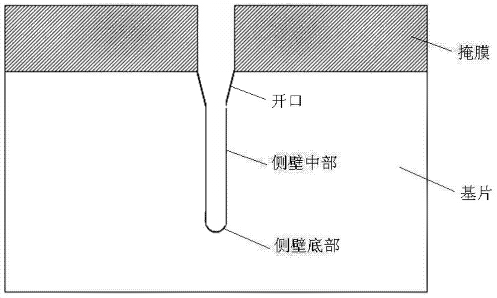
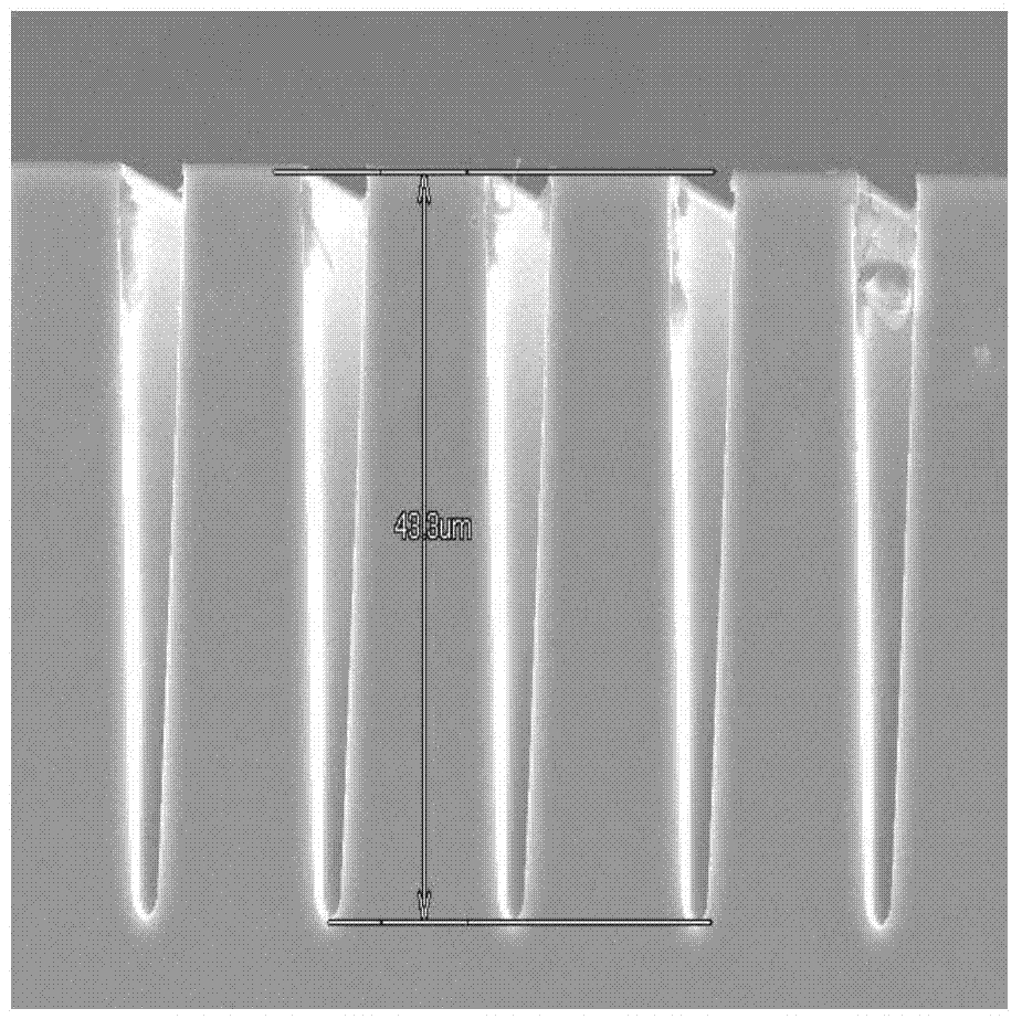
[0002] In recent years, with MEMS devices and systems being more and more widely used in the fields of automobiles and consumer electronics, and the broad prospects of TSV (Through Silicon Etch, through hole etching) in the future packaging field, deep silicon etching technology has gradually become One of the hottest processes in the field of MEMS processing and TSV technology. Moreover, for different applications, there are different requirements for the substrate morphology obtained by the deep silicon etching process. Requirements, and in order to ensure the performance and stability of the device, it is required that the top opening of the trench is inclined to be V-shaped, the middle and bottom of the side wall are steep, and the bottom surface is smooth, such as figure 1 shown.

[0003] An existing substrate et...

Examples

Embodiment Construction

[0034] In order for those skilled in the art to better understand the technical solution of the present invention, the substrate etching method provided by the present invention will be described in detail below in conjunction with the accompanying drawings.

[0035] image 3 A flow chart of the substrate etching method provided by the present invention. see figure 1 , the method includes the following steps:

[0036] S1, feed etching gas, passivation gas (also known as protective gas) and auxiliary gas into the reaction chamber, and turn on the excitation power supply (such as radio frequency power supply), and the excitation power supply applies excitation power to the reaction chamber to make the reaction chamber The etching gas is excited to form plasma; the bias power supply is turned on, and the bias power supply applies bias power to the substrate, so that the plasma etches the substrate until a predetermined etching depth is etched on the substrate. Moreover, in thi...