Transistor and manufacturing method thereof

A manufacturing method and transistor technology, applied in semiconductor/solid-state device manufacturing, semiconductor devices, electrical components, etc., can solve the problems of small and complex carrier mobility in the channel region, and achieve the effects of simplified manufacturing process and good compatibility

Inactive Publication Date: 2015-07-01
SEMICON MFG INT (SHANGHAI) CORP
View PDF3 Cites 15 Cited by
  • Summary
  • Abstract
  • Description
  • Claims
  • Application Information

AI Technical Summary

Problems solved by technology

[0006] However, the existing NWFET technology has the problem of low carrier mobility in the channel region, and some manufacturing methods for improving carrier mobility in the prior art are relative

Method used


Image

  • Transistor and manufacturing method thereof
  • Transistor and manufacturing method thereof
  • Transistor and manufacturing method thereof

Examples


Example Embodiment

[0017] Although the nanowire field effect transistor in the prior art suppresses the short channel effect, the carrier mobility in the channel region of the transistor in the prior art does not meet the requirements, and the performance of the transistor is not good enough.

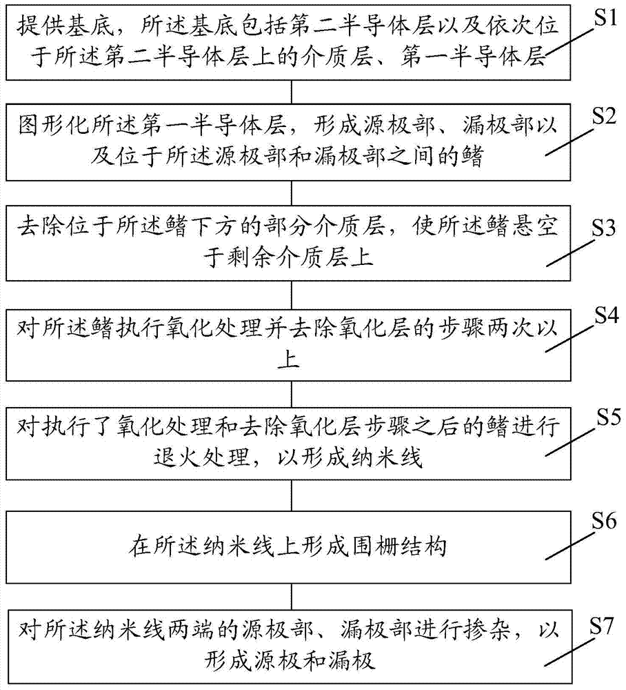
[0018] In order to solve the problems of the prior art, the present invention provides a method for manufacturing a transistor. refer to figure 1 , showing a schematic flow chart of an embodiment of the method for manufacturing a transistor of the present invention. The manufacturing method generally includes the following steps:

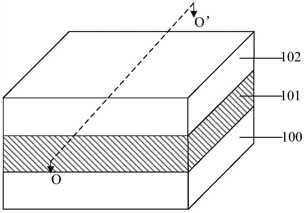
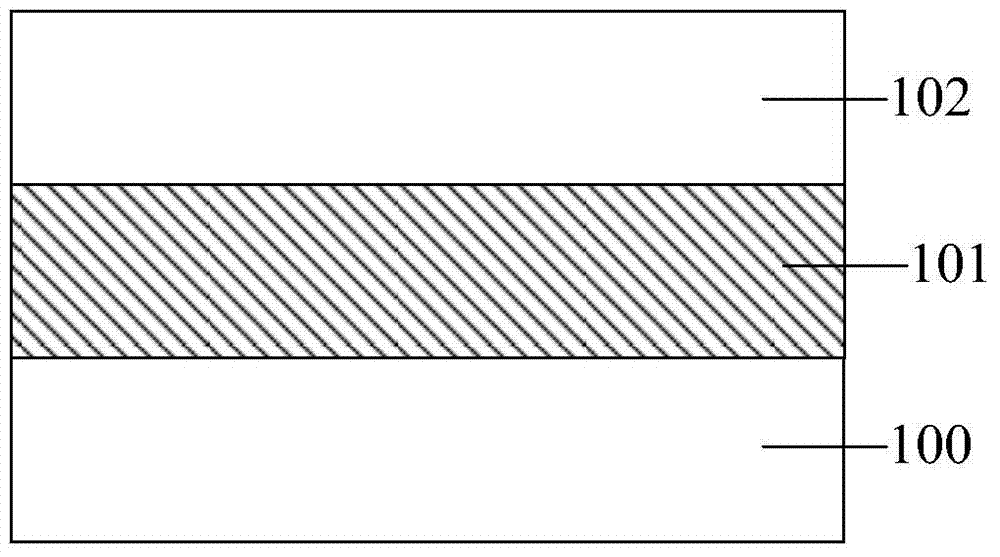
[0019] Step S1, providing a substrate, the substrate comprising a second semiconductor layer, a dielectric layer and a first semiconductor layer sequentially located on the second semiconductor layer;

[0020] Step S2, patterning the first semiconductor layer to form a source portion, a drain portion, and a fin between the source portion and the drain portion;

[0021] Step ...


PUM

PropertyMeasurementUnit
Thicknessaaaaaaaaaa
Diameteraaaaaaaaaa
Lengthaaaaaaaaaa

Abstract

The invention provides a transistor and a manufacturing method thereof. The manufacturing method comprises the following steps: patterning a first semiconductor layer and forming a source part, a drain part and a fin between the source part and the drain part; removing part of a dielectric layer and making the fin suspended on the remaining dielectric layer; performing the step of oxidizing the fin and removing an oxide layer twice or more to form a nanowire; and forming a fence structure on the nanowire. The transistor comprises a substrate, a germanium nanowire, and a fence structure. The substrate comprises a silicon layer, and a dielectric layer and a germanium-silicon layer disposed on the silicon layer sequentially. A groove is formed in the germanium-silicon layer and part of the dielectric layer, and the parts of the first semiconductor layer at the two sides of the groove are respectively used as a source or a drain. The germanium nanowire is disposed between the source and the drain and is in contact with the source and the drain. The fence structure fills the groove and covers the nanowire. According to the invention, the carrier mobility of the channel region of the transistor can be improved, and the performance of the transistor can be optimized.

Description

technical field [0001] The present invention relates to the technical field of semiconductors, and in particular, to a transistor and a manufacturing method thereof. Background technique [0002] In order to keep up with Moore's Law, the feature size of semiconductor devices is gradually decreasing. Improving performance by shrinking the physical size of conventional field-effect transistors has faced some difficulties because the switching performance of transistors is degraded by short channel effects and gate leakage issues at small sizes. [0003] In order to suppress the short-channel effect, the prior art has developed a Nanowire Field-Effect Transistor (NWFET) technology. [0004] The NWFET has a one-dimensional nanowire channel, usually using a gate-wrap structure, and the gate can modulate the one-dimensional nanowire channel from multiple directions, thereby enhancing the modulation capability of the gate and improving the threshold characteristics. [0005] It c...

Claims


Application Information

Patent Timeline
IPC IPC(8): H01L21/335H01L29/775B82Y10/00
Inventor 肖德元
Owner SEMICON MFG INT (SHANGHAI) CORP
Why Eureka
Try Eureka