Semiconductor structure forming method

A semiconductor and gate structure technology, applied in the field of semiconductor structure formation, can solve problems such as unstable performance of fin field effect transistors

Inactive Publication Date: 2015-07-01
SEMICON MFG INT (SHANGHAI) CORP
View PDF6 Cites 4 Cited by
  • Summary
  • Abstract
  • Description
  • Claims
  • Application Information

AI Technical Summary

Problems solved by technology

[0006] However, the prior ar...

Method used


Image

  • Semiconductor structure forming method
  • Semiconductor structure forming method
  • Semiconductor structure forming method

Examples


Embodiment Construction

[0038] As mentioned in the background, the performance of the prior art FinFET is not stable.

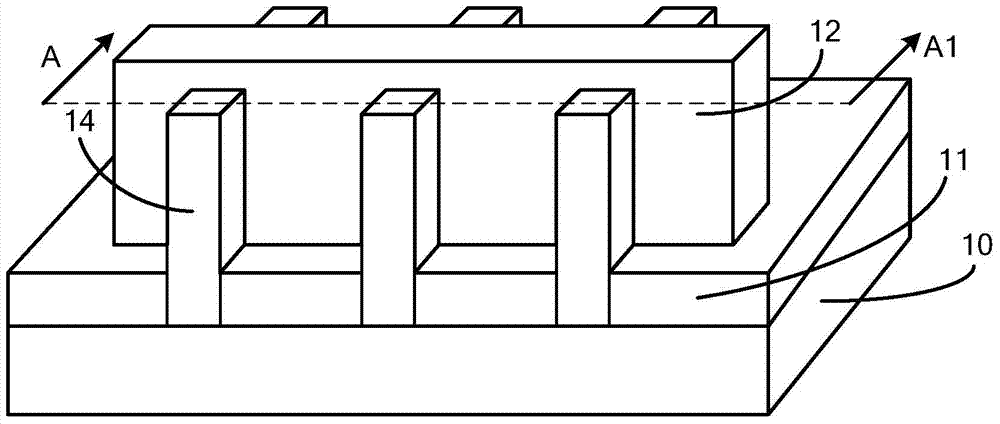
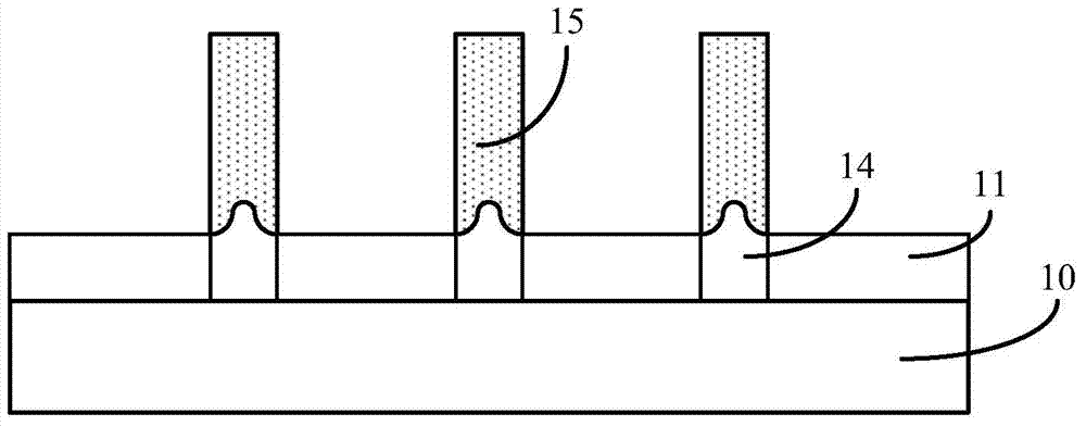
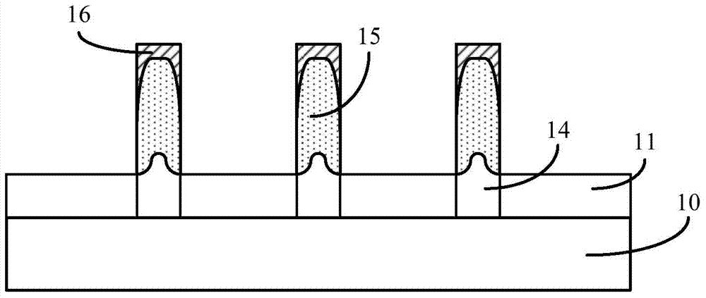
[0039] After research, please continue to refer to figure 2 , figure 2 yes figure 1 Schematic diagram of the cross-sectional structure along the AA1 direction. For a fin field effect transistor, it is necessary to adopt an ion implantation process in the gate structure 12 (such as figure 1 As shown), the fins 14 on both sides are doped with P-type ions or N-type ions to form source regions and drain regions 15, and the top and sidewalls of part of the fins 14 covered by the gate structure 12 need to become Therefore, the ion implantation process needs to dope both the top and the sidewall of the fin 14 , so that both the sidewall and the bottom of the fin 14 can form the source region and the drain region 15 .

[0040] However, since the ion implantation process needs to dope both the sidewall and the top of the fin portion 14, the ion implantation energy received by the fin port...


PUM


Abstract

A semiconductor structure forming method comprises providing a semiconductor substrate, wherein a doping region is arranged in the substrate; performing laser ion injection process on the doping region, wherein the laser ion injection process comprises performing ion injection on the doping region to enable doping ions to be arranged in the doping region; performing laser processing on the doping region to heat the doping region and eliminate ion injection damage. By the aid of the method, the structural performance of the formed semiconductors is improved.

Description

technical field [0001] The invention relates to the technical field of semiconductor manufacturing, in particular to a method for forming a semiconductor structure. Background technique [0002] With the rapid development of semiconductor manufacturing technology, semiconductor devices are developing towards higher element density and higher integration. As the most basic semiconductor device, semiconductor structure is currently being widely used. Therefore, with the increase of component density and integration of semiconductor devices, the gate size of planar semiconductor structure is getting shorter and shorter. The traditional planar semiconductor structure has a great influence on channel current. The control ability of the semiconductor is weakened, resulting in short channel effect, resulting in leakage current, and finally affecting the electrical performance of semiconductor devices. [0003] In order to overcome the short channel effect of the semiconductor stru...

Claims


Application Information

Patent Timeline
IPC IPC(8): H01L21/336H01L21/265
CPCH01L21/265H01L21/268H01L29/66795
Inventor 禹国宾
Owner SEMICON MFG INT (SHANGHAI) CORP
Why Eureka
Try Eureka