Method for manufacturing semiconductor device

A manufacturing method and semiconductor technology, applied in semiconductor/solid-state device manufacturing, electrical components, circuits, etc., can solve problems such as large chipped corners, affecting the electrical performance of semiconductor devices, and sharp tops of shallow trench isolation structures, etc., to achieve improved Smoothness, improve the performance of semiconductor devices, prevent the effect of uneven electric field

Inactive Publication Date: 2015-07-01
SEMICON MFG INT (SHANGHAI) CORP
View PDF7 Cites 1 Cited by
  • Summary
  • Abstract
  • Description
  • Claims
  • Application Information

AI Technical Summary

Problems solved by technology

The two larger notch 121 will form a cusp 122 in the middle of the top of the shallow trench isolation structure. The larger the width of the notch 121, the sharper the cusp 122. The larger notch 121 and the sharp cusp 122 are in the semiconductor Many problems will be caused in the subsequent manufacturing process of the device, which will affect the electrical performance of the final semiconductor device
[0006] For this reason, a new method of manufacturing semiconductor devices is needed to solve the problem of large chipping at the top side edge of the shallow trench isolation structure when removing the pad oxide layer, and resulting in the formation of the top middle of the shallow trench isolation structure. sharp-edged problem

Method used


Image

  • Method for manufacturing semiconductor device
  • Method for manufacturing semiconductor device
  • Method for manufacturing semiconductor device

Examples


Embodiment Construction

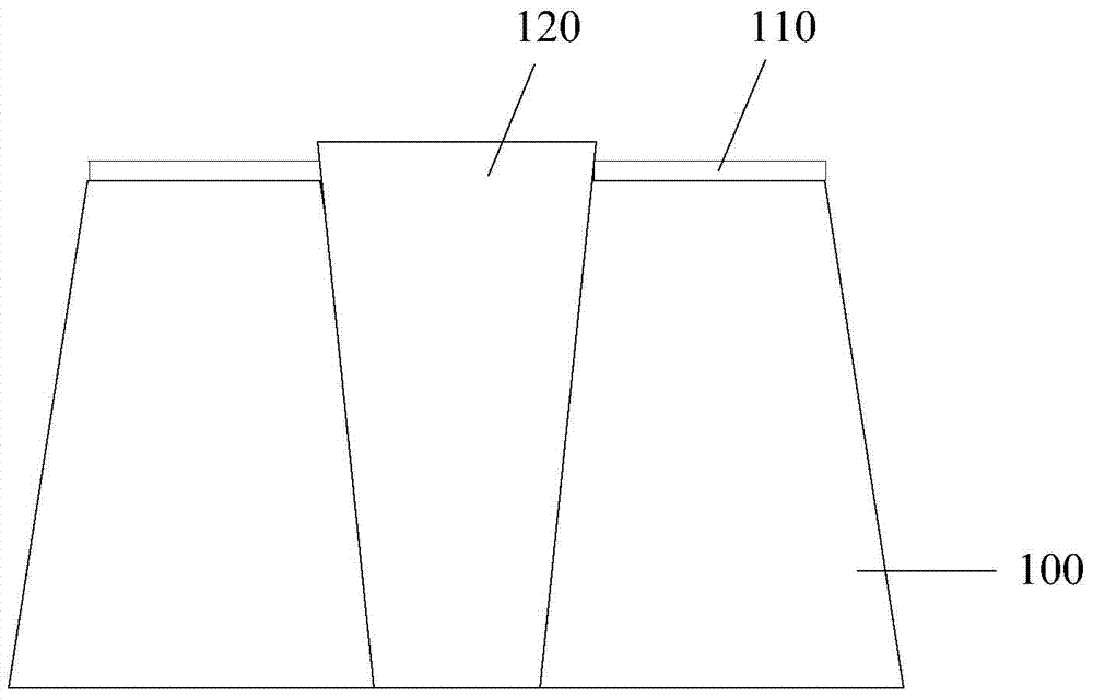
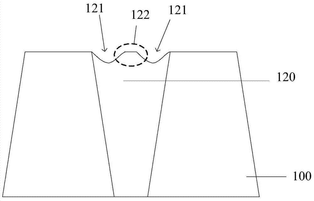
[0034] As mentioned in the background technology, the existing semiconductor device manufacturing method uses a wet etching process to remove the pad oxide layer on the semiconductor substrate. The wet etching process will not only etch the pad oxide layer, but also the shallow trench The insulating material of the isolation structure is etched, because the top side edge of the shallow trench isolation structure is easily wetted by the wet etching solution, so the top side edge of the shallow trench isolation structure is easy to be etched into a large missing corner. And because the wet etching process is an isotropic etching process, the width of the larger notch is usually twice the depth, that is, the width of the notch is larger, resulting in a gap between the top and middle of the shallow trench isolation structure. Form sharp cusps. The sharp protrusions will lead to uneven surface of each layer structure subsequently formed on the shallow trench isolation structure, re...


PUM


Abstract

A method for manufacturing a semiconductor device comprises the following steps: providing a semiconductor substrate on which a pad oxide layer is formed; forming a shallow trench isolation structure in the semiconductor substrate, wherein the top of the shallow trench isolation structure is higher than the surface of the semiconductor substrate; and simultaneously removing the pad oxide layer and the part, higher than the surface of the semiconductor substrate, of the shallow trench isolation structure by an anisotropic etching process, wherein etching gases adopted by the anisotropic etching process contain NF3 and also contain at least one of NH3 and H2. The anisotropic etching process adopting NF3 and NH3 (H2) can reduce the roughness of the surface after etching. The trench isolation structure has a flat top, and no sharp bulge is produced. Thus, sharp bulges are prevented from being produced on the surfaces of structures subsequently formed on the shallow trench isolation structure, adverse consequences such as an uneven electric field or tip discharge are prevented, and the performance of the semiconductor device is improved eventually.

Description

technical field [0001] The invention relates to the field of semiconductor manufacturing, in particular to a method for manufacturing a semiconductor device. Background technique [0002] As the size of integrated circuits decreases, the devices that make up the circuits must be placed more densely to fit the limited space available on the chip. Since current research is devoted to increasing the density of active devices per unit area of ​​a semiconductor substrate, effective insulating isolation regions between circuits become more important. The methods for forming isolation regions in the prior art mainly include local oxidation isolation (LOCOS) process or shallow trench isolation (STI) process. The Shallow Trench Isolation (STI) structure has the advantages of various manufacturing processes and good electrical isolation performance, including reducing the area occupied by the surface of the silicon wafer while increasing the integration of devices, maintaining surfac...

Claims


Application Information

Patent Timeline
Patent Type & Authority Applications(China)
IPC IPC(8): H01L21/762
CPCH01L21/76224H01L21/31116
Inventor 潘周君
Owner SEMICON MFG INT (SHANGHAI) CORP
Why Eureka
Try Eureka